Suitable for microfabrication of sapphire, diamond, and ceramics
Overview: What is a UV laser?
Lasers are broadly classified as either continuous wave (CW) lasers that emit light continuously, or pulse lasers that emit light in pulses. Development on lasers for micromachining has two main streams: one is shortening the laser wavelength, and the other is shortening the laser pulse duration.
UV lasers are part of the stream focused on shortening the laser wavelengths. Our company's 355nm wavelength UV laser can perform more precise fabrication than longer wavelength lasers like YAG and CO2 lasers.
Classification of UV lasers

Advantages of UV laser processing
The UV laser has two main advantages compared to longer wavelength lasers.
1. It is possible to process more precisely, since the focus diameter can be made smaller when using a focusing lens.
Generally, the minimum diameter of a focused laser is approximately the same as its wavelength. Therefore, a shorter wavelength laser makes it possible to fabricate more precise structures, which is why development on the laser oscillator is directed towards shortening the laser wavelength.
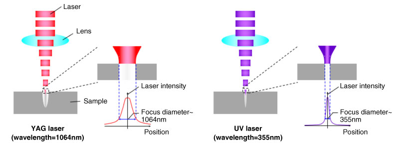
2. Efficient laser processing is possible, since the photon energy is high.
Generally, the photon energy is inversely proportional to its wavelength. Therefore the shorter the wavelength, the higher the energy.
This is another reason why development on the laser oscillator has trended towards shorter laser wavelengths.
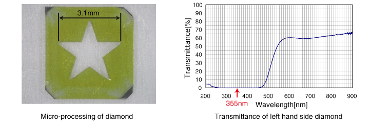
Even diamond, the hardest material in the world, can be processed because it directly absorbs UV laser energy.
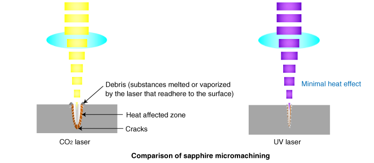
Sapphire cannot be processed by a YAG laser since the photon energy is not high enough to cause absorption. Although a CO2 laser can cause absorption through the lattice vibration of the crystal, it can leave many cracks and heat affected zones due to the thermal processing.
However, since the UV laser has high photon energy, by using a focusing lens, absorption occurs and processing can be accomplished.
Features of Orbray's UV laser micromachining
We have been using laser processing for many years to cut diamonds in the production of diamond styluses, as well as to drill sapphire, ruby and ceramics.
Since customer requests for smaller diameter holes have increased in recent years, we introduced the UV laser (wavelength: 355nm) earlier than other manufactures in order to provide precision micromachining.
Our company's core technology (cutting, grinding and polishing) has been built on processing hard materials, and we can offer the best solutions for materials such as sapphire, ruby, diamond and ceramics. Materials can be polished after laser micromachining for final finishing.
Position of the UV laser among other microfabrication technologies
This table compares UV laser micromachining with other microfabrication processes. For the purposes of comparison, the example used in the table is micro-hole processing in sapphire, which our company has mass-produced.
Microfabrication processes |
Minimum diameter |
Maximum aspect ratio |
Surface roughness |
Damaged area by processing |
Tapered or non-tapered surface |
|---|---|---|---|---|---|
Ultrasonic processing |
500μm |
10 |
Rough |
Exist |
Non-tapered |
CO2 laser |
500μm |
10 |
Rough |
Exist |
tapered |
Drilling |
150μm |
4∼20 |
Rough |
Exist |
Non-tapered |
Sand blast |
100μm |
2∼4 |
Rough |
Exist |
Tapered |
UV laser |
60μm |
30 |
Smooth |
Small |
Non-tapered |
0.5μm |
20 |
Smooth |
Very small |
Non-tapered |
|
Dry etching |
0.01μm |
1 |
Very smooth |
None |
Non-tapered |

Sapphire is a hard, brittle material that breaks easily, and it is very difficult to form micro-holes in it - especially holes with a diameter less than 100µm. Ultrasonic processing and CO2 lasers can only produce holes with a minimum diameter of 500µm. And when it comes to mechanical drilling, the drill itself is hard to create, and the smallest possible diameter is still only 150µm. Moreover, multiple holes cannot be fabricated consecutively due to the frictional wear on the drill.
Sandblasting can form 100µm diameter holes but the aspect ratio is limited to 2-4 due to the limits of mask durability. In addition, all four of these fabrication processes often cause micro cracks around the hole.
By comparison, our company's UV laser can achieve a minimum diameter of 60µm and maximum aspect ratio of 30.
Our processing machine is equipped with a special optical system which can irradiate material with the laser in an extremely short time.
Therefore, a smooth processed surface can be obtained with minimal heat effect. The actual surface roughness Ra is 0.5μm. Additionally, while laser processing usually leaves the material surface with a tapered wall, our machine can give the surface a perpendicular wall.
Moreover it is possible to polish the surface of the hole by combining our core technologies of cutting, grinding, and polishing.


To fabricate a smaller diameter hole, the femtosecond laser can be selected. The minimum diameter possible is 0.5µm and the maximum aspect ratio is 20. Please refer to the femtosecond laser in detail. Dry etching can create extremely small nano-holes, but due to the limits of photoresist's durability, the maximum depth of the hole is limited to 1 times the hole diameter. Moreover, since engineering designs change frequently during the prototyping stage, the additional photomasks required for each change add to the initial cost. We have a proven track record of producing both engineering samples and mass production quantities of precision industrial and consumer parts. We are able to manufacture complex shapes using CAD data and numerical control. We work with our customers starting from the design stage, to test samples, to mass production. We can also process customer-supplied materials. Please do not hesitate to contact us for your micromachining needs.
UV laser machining capability
In the case of sapphire processing, the laser machining capability is as follows:
<Micro-hole processing>
- Minimum diameter: 60µm
- Maximum aspect ratio: 30
- Surface roughness: Ra=0.5µm
(with UV laser processing)
<Micro structures>
- Minimum processing line width: 100µm
- Maximum aspect ratio: 10
- Surface roughness: Ra=0.5µm
(with UV laser processing) - Maximum sample size: 300mm x 200mm
Applications and examples
Sapphire via wafer
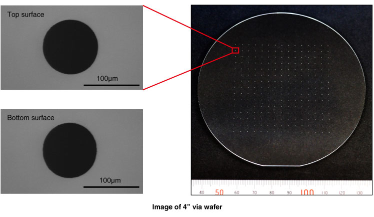
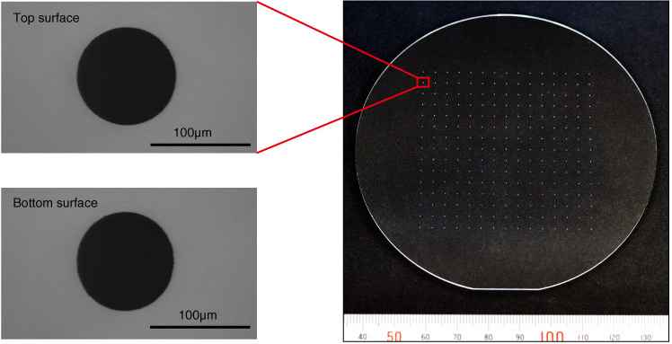
225 φ100μm micro-holes in a 4-inch, 0.5mmt sapphire wafer. Used for through-sapphire via.
High aspect ratio micro-hole in sapphire
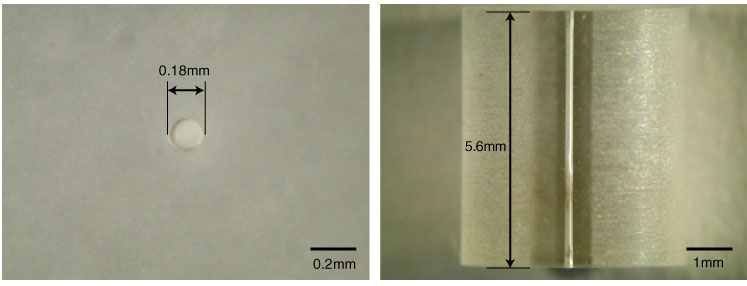
A hole with extremely high aspect ratio: diameter φ0.18mm, length 5.6mm, aspect ratio 31. Used for precision parts of manufacturing machinery.
Star-shaped diamond
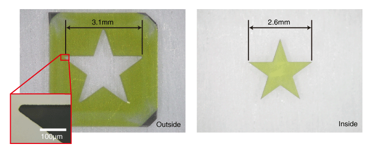
Star-shaped cut-out in 0.7mm thick diamond. Sharp corners are cleanly processed.
Surface roughness of laser cut diamond
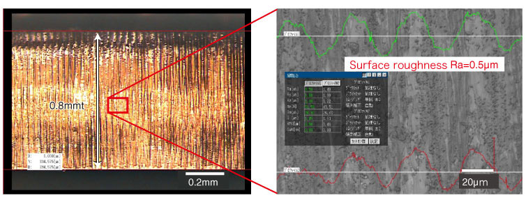
In the case of the diamond, a smooth surface with average surface roughness Ra of 0.5μm can be obtained.


