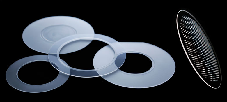
NAPHIA™ sapphire is used in semiconductor processing as a carrier wafer, such as for a support in the
handling of ultra-thin device wafers. Utilizing the polishing technology we have cultivated over many years,
we are able to manufacture ultra-large support wafers and carrier plates with a diameter of up to 12 inches
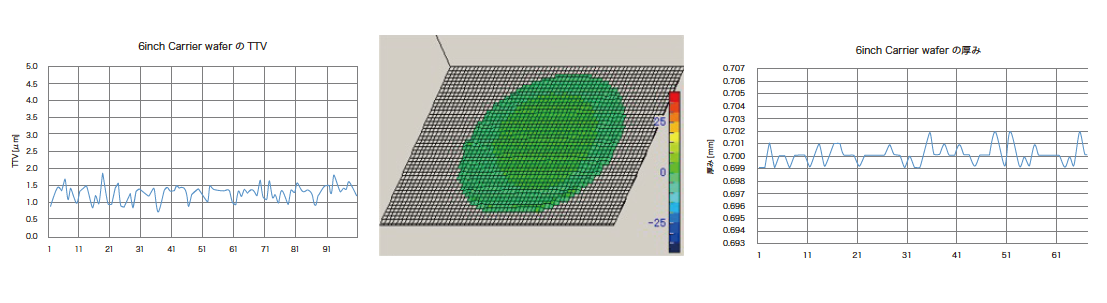
(300mm). The TTV of carrier wafers is a critical parameter, and our carrier wafer has best-in-class minimal
TTV.
Furthermore, we have the capability of additional processing, such as drilling and grooving, which is
available for all specifications. We also offer adapter wafers, which allow the use of small wafers in
equipment designed for large wafers.
Compared to glass/ceramics, sapphire has excellent heat, chemical, and plasma resistance, so it can be used
in high-temperature processes or harsh environments without distortion or deformation.
Features of sapphire carrier plates
- No contamination
- High degree of flatness
- High hardness
- High heat resistance
- Highly insulating
- Processing such as drilling is possible, and it can be transported by suction
- Corrosion resistance
- Option: Sapphire vacuum chuck with through holes
| Item | Specification | ||||
|---|---|---|---|---|---|
| Diameter | φ4 inch | φ5 inch | φ6 inch | φ8 inch | φ12 inch |
| Material | Artificial sapphire( Al2O3 99.99%以上) | ||||
| Thickness | 1±0.003mm | 3±0.005mm | |||
| Orientation | c-plane ( 0001 ) / r-plane ( -1012 ) | c-plane ( 0001 ) | |||
| OF | Flat / Notch / None | ||||
| TTV | ≦2.5μm | ≦3.0μm | |||
| Front side finishing | Polish (Ra<0.3nm) | ||||
| Back side finishing | Polish (Ra<0.3nm) | ||||
| Remarks | Customizable specifications: thickness, orientation, single-side polishing. Other options: drilling, laser marking, delivery by thickness classification, re-polishing |
||||