To solve the problems faced by optical fiber polishing, we have developed a new optical fiber laser processing technology using a laser beam. We will compare polishing and laser processing and explain the laser forming technology (Laser-FT™) we have developed.
Challenges in Polishing Process
- Visual inspection process cannot be eliminated.
- Cleaning process cannot be eliminated.
- It is difficult to automate the entire process from bonding to polishing of optical fibers.
- It is difficult to polish an optical fiber by itself.
Comparison of Polishing And Laser Processing
| Polishing processing | Laser processing | |
| Pros |
|
|
| Cons |
|
|
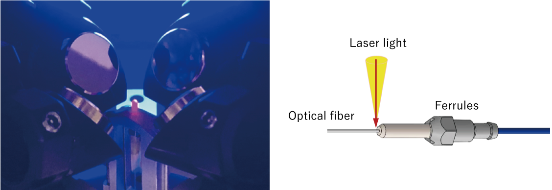
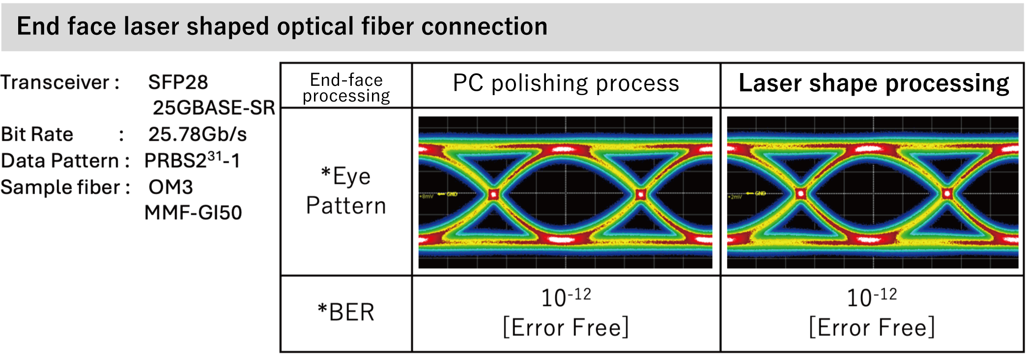
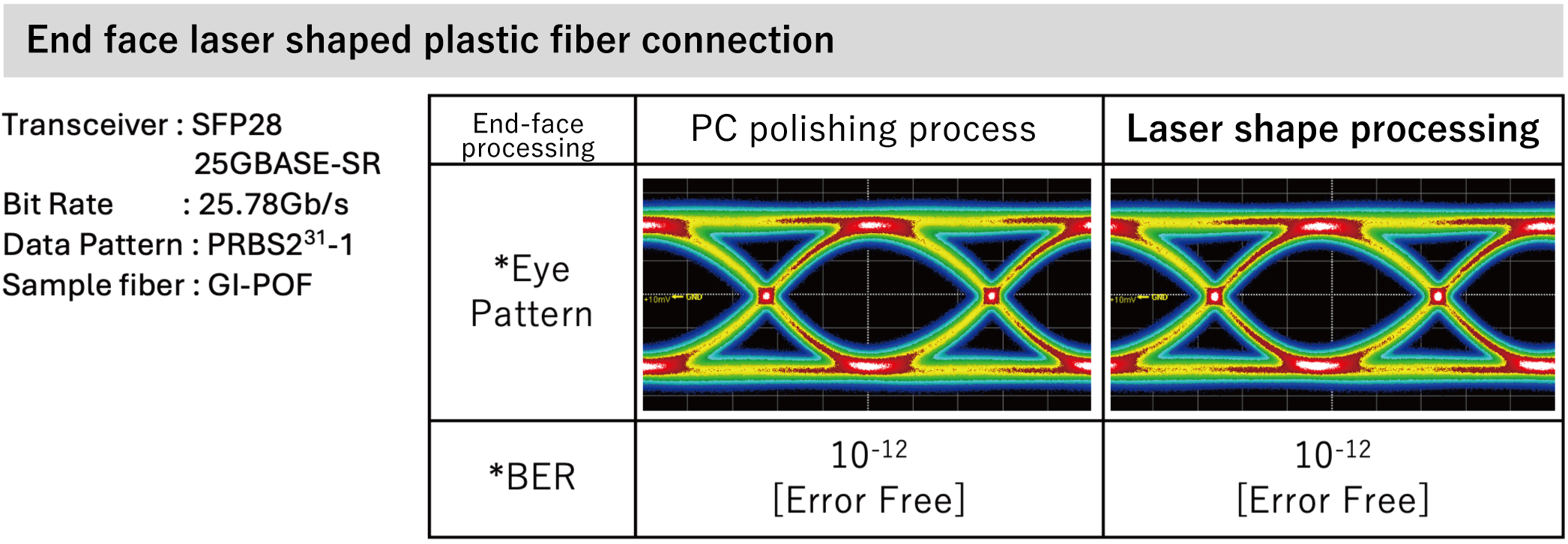
Laser forming for Optical Fiber Connection
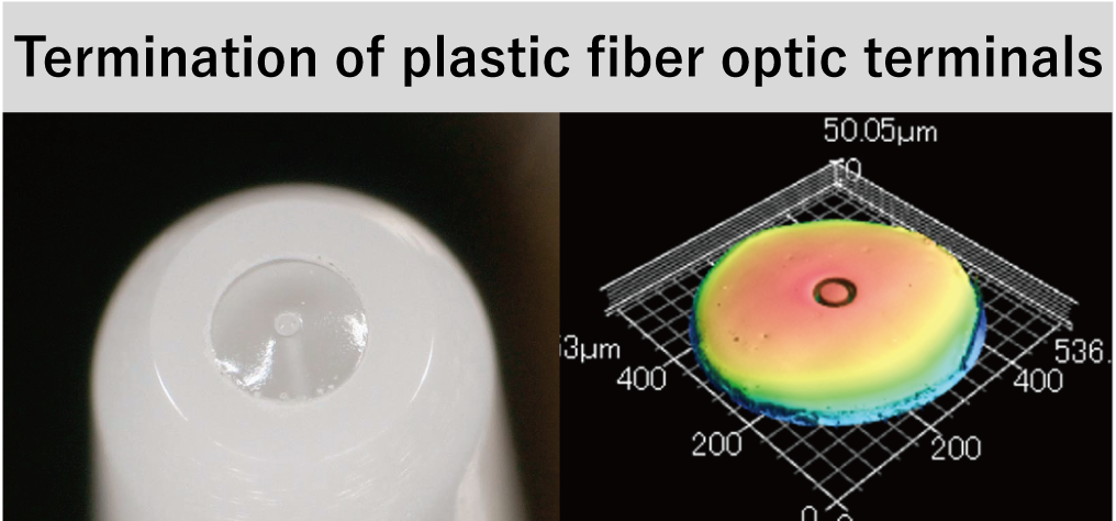
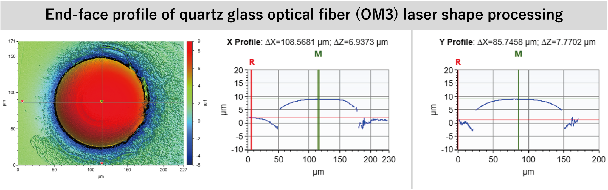
Laser forming equipment uses a laser light source most suitable for optical fiber processing and incorporates an optical lens system that adjusts the beam quality for microprocess of ultrafine optical fibers, enabling processing of both quartz glass optical fibers and plastic optical fibers. The end surface of the optical fiber is formed into a uniform convex shape, resulting in a smooth surface with no flaws, and can obtain optical performance that is equal to that of a polished fiber.
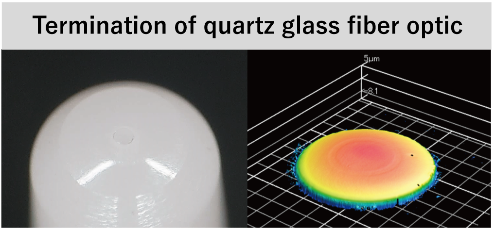
Feature 1) Well-Proportioned Optical Fiber End-Face, Smooth Surface Without Flaws
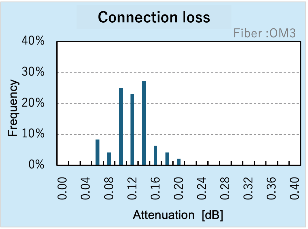
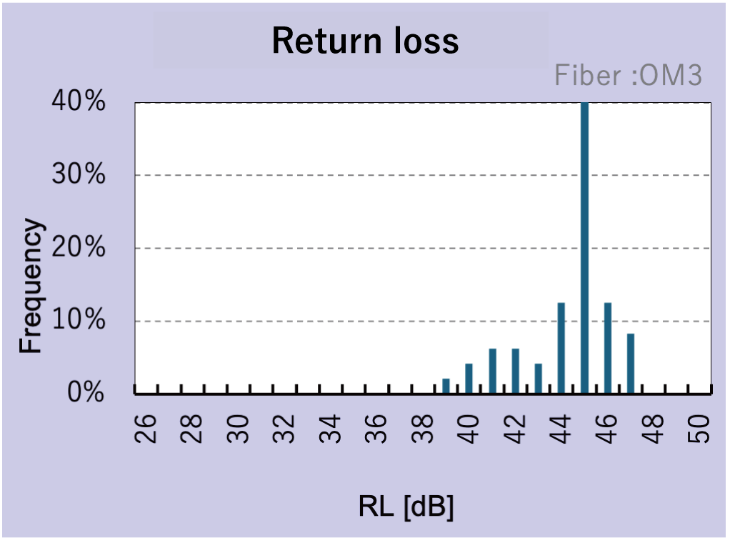
Feature 2) Stable Optical Performance When Connected
Feature 3) Compatible With Multi-Gigabit Optical Communications
References
IEEE P802.3cz Multi-Gigabit Optical Automotive Ethernet Task Force Sept.2020
End Face Termination for Butt Coupling (GI-POF)
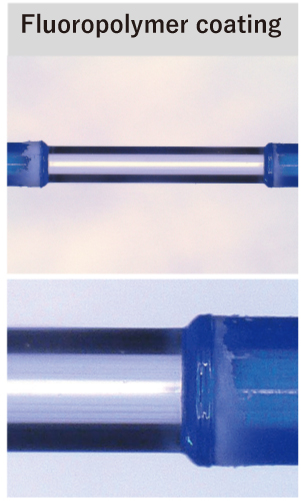
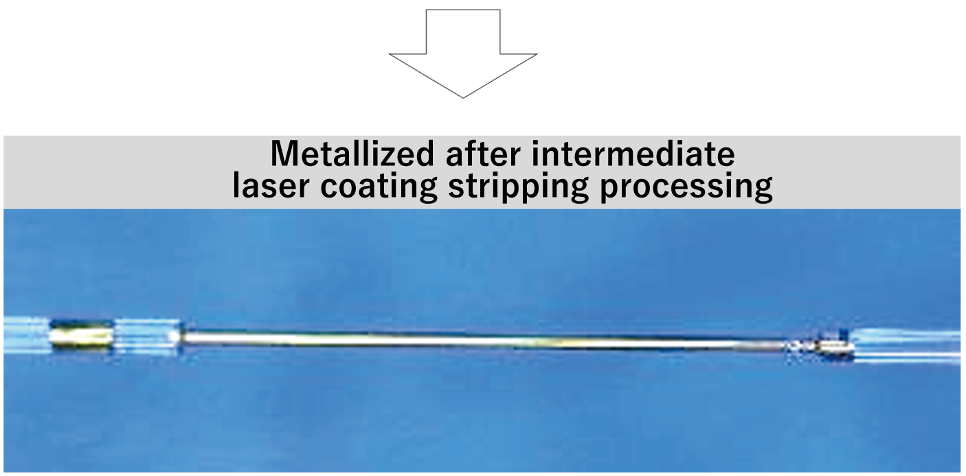
Laser Stripping of Optical Fibers
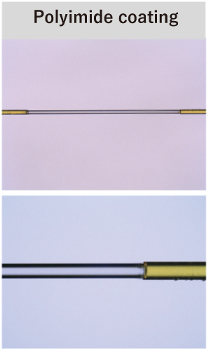
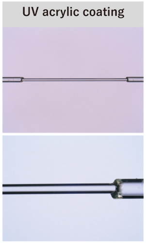
The coating material protects the optical fiber from the operating environment, and the laser stripping process can be used to remove a variety of coating materials.
For example, polyimide is often used as a coating material for optical fibers used in medical equipment due to its heat resistance and chemical resistance.
However, its characteristics make it difficult to remove by heating and melting. Therefore, it is currently removed by heating and immersing it in a hazardous chemical.
With laser stripping, the energy required to break down the bonded part of the polyimide resin can be applied in a very short period of time, allowing for easy removal of the coating.
Furthermore, we can also offer intermediate stripping, and stripping length and position can be controlled with high precision. In addition, while mechanical removal methods may damage the glass surface, our laser removal method reduces damage to the optical fiber, resulting in a smooth strip surface. This can also be expected to stabilize the adhesion of the metallization process to the outer fiber diameter.
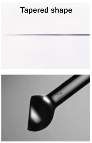
Optical Fiber Lens by Laser forming
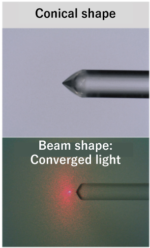
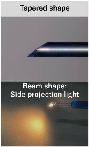
Laser forming can be used to process the tip of an optical fiber into a wedge shape, a conical shape, or a beveled/tip-angled shape. This enables the beam shape emitted from the optical fiber to be formed into any desired shape. This lens processing of optical fibers is expected to be used in various fields such as silicon photonics interconnections, in-vehicle (Automotive?) communications, medical equipment, and sensor applications. We will propose the optimum shape to meet your specifications.

Applications:
Photonic devices
Applications:
Riding, medical devices
Applications:
Silicon photonics, sensing
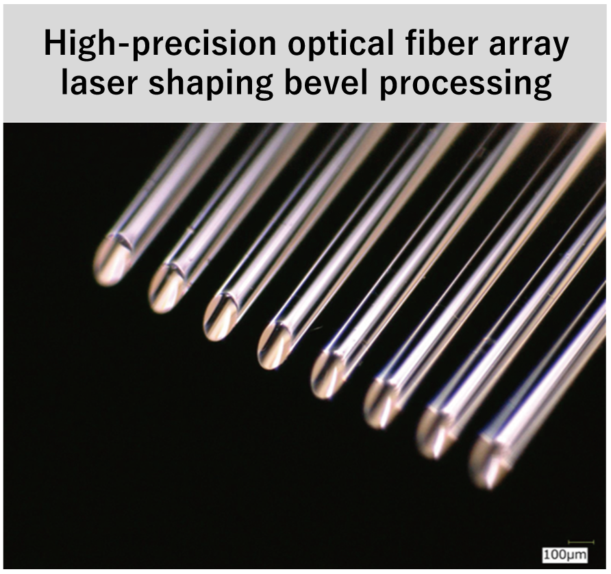
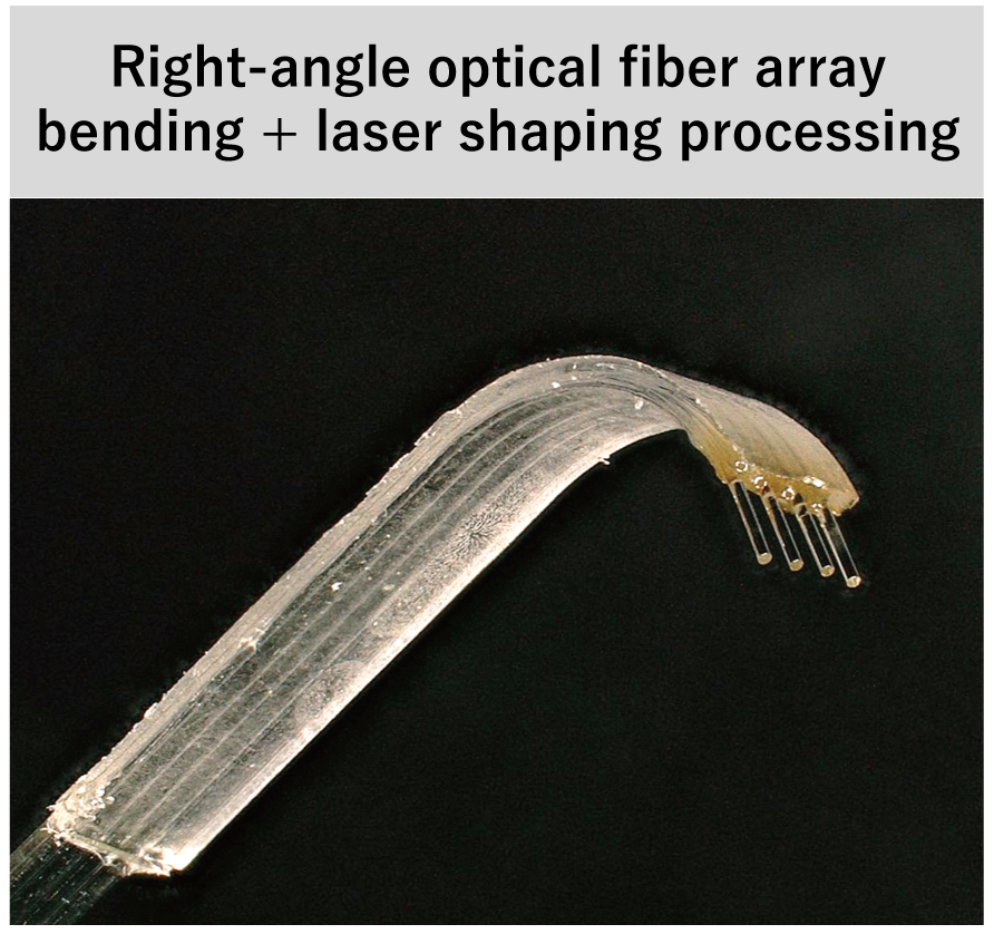
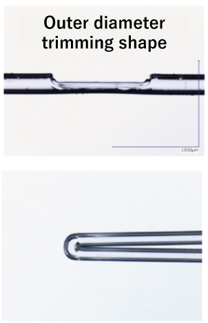
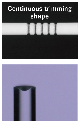
Other Fiber Optic Customized Processing Examples
Special Processing Technology Draws Attention in Connection of Photonics-Electronics Convergence
The next-generation optical interface in the IOWN® concept proposed by NTT requires high-speed and low-power consumption to handle large amounts of traffic, and Photonics-Electronics Convergence are attracting attention as the core technology to realize these requirements. The Photonics-Electronics Convergence devices require packaging technologies that enable high-density integration of various devices, such as silicon photonic waveguides and VCSEL/PD chip arrays.
Orbray has the technology to precisely align optical fibers with these densely integrated devices, and by combining this alignment technology with laser forming, we are contributing to the development and progress of Photonics-Electronics Convergence devices. For example, we are capable of performing fiber tip processing, which aligns the end faces of optical fibers with high precision and applies an arbitrary angle to all optical fibers, and optical fiber array processing, which converts optical fibers from vertical to horizontal by bending them, as in the case of light angles.
*"IOWN®" is a trademark or registered trademark of NTT(Nippon Telegraph and Telephone Corporation).
*IOWN® is also introduced(described) on the following pages.
High-precision processing technology for photoelectric fusion devices and silicon photonics