We offer contract polishing services, such as optical substrate end face polishing used in silicon photonics for specific polishing amounts, using our high-quality polishing process and services as follows.
-
Substrate cutting process
Cutting to specified dimensions is available before or after polishing of the end face.
The cutting process is available for both wafer and bar conditions. -
Fixing process using a dedicated jig fixture
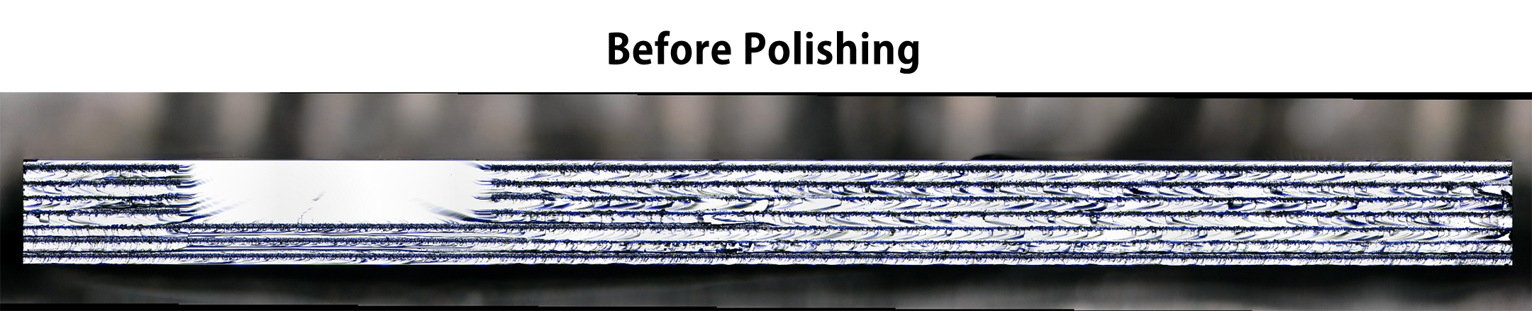
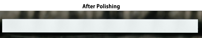
The polishing jig is designed in-house in accordance with the size of the optical substrate. The substrate is fixed by adhesive and processed in a stable condition and thus, enables high-precision polishing. -
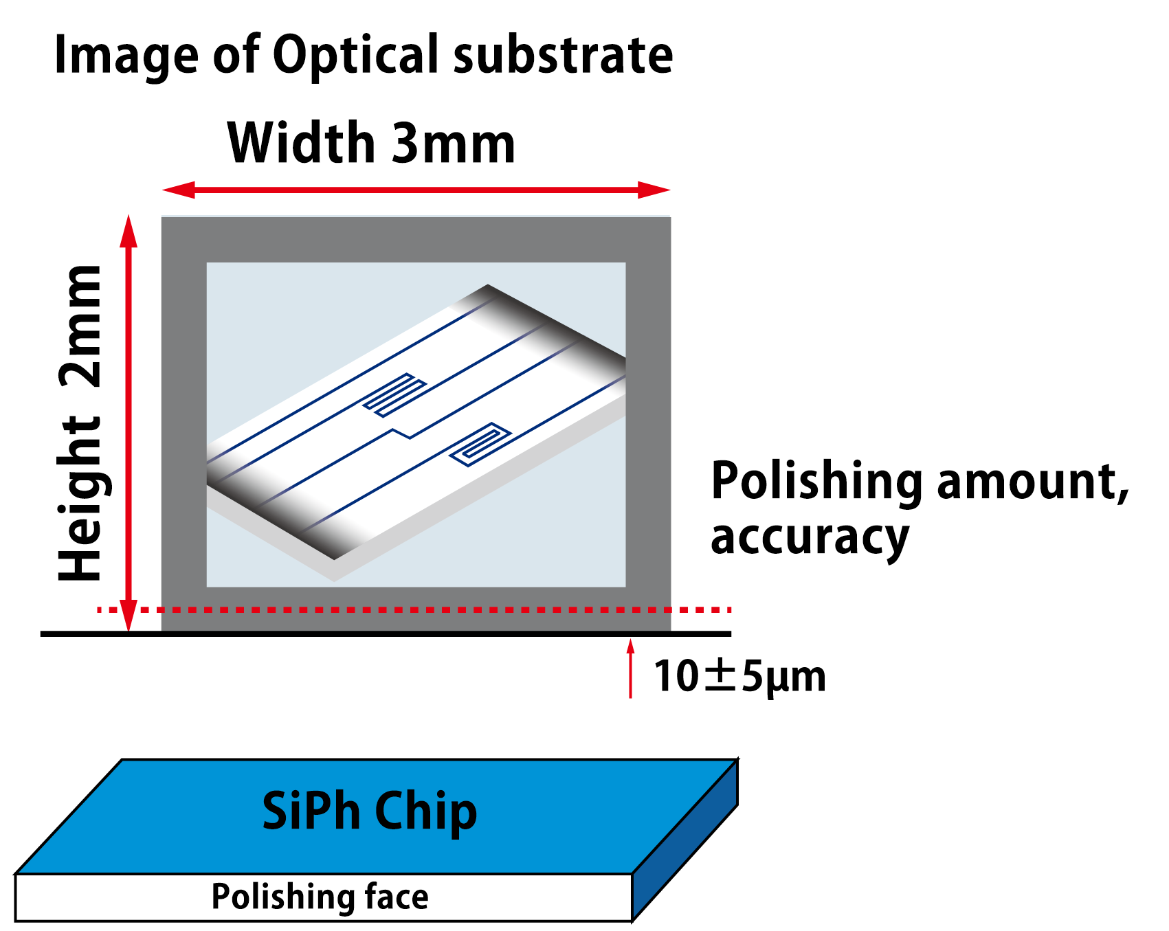
Polishing amount and accuracy
Polishing of 10μm or more is assumed, with a polishing accuracy of ±5μm.
We also offer custom products, ensuring a high quality of polishing quantity and accuracy according to requirements. -
Material
We can process materials such as Silicon (Si) and Lithium Niobate (LN) Sapphire.
We provide the most suitable polishing process for each material characteristic to meet the requirements of our customers. We can consider the use of other materials as well. -
AR Coating, Cleaning substrates
We offer AR (Anti-reflection)Coating and cleaning process in accordance with the material substrates.
This maintains the quality of the substrate surface after polishing and provides the best substrate for various applications.
We provide high-quality end-face polishing of optical substrates by utilizing our cutting-edge technology and extensive experience. Our flexible response to customer needs and reliable quality control ensures highly reliable services. Please feel free to contact us at any time for any questions or consultation.
Our experience in processing Si/LN Substrates
| Substrate design | Width | Height | Thickness | Polishing |
|---|---|---|---|---|
| 2~25mm | 1~20mm | 1.5mm or lower | 0 deg、8deg or etc. |
- Dicing Process
- Polishing accuracy ±5µm
- Experience and know-how Si, LN, etc.…
- AR Coating
- Cleaning of Substrates
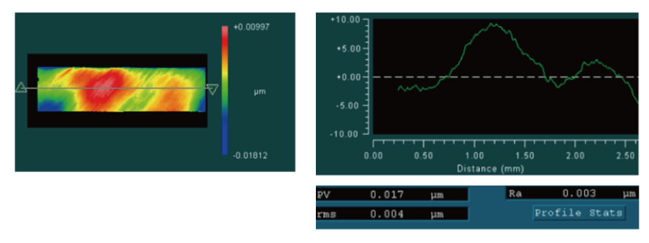
Surface Roughness
・Ra0.1µm
Surface Roughness(Zygo)