For information regarding our journey from "Adamant Namiki Precision Jewel Co." to "Orbray Co." Please click here

Ceramic wafers
NAPHIA

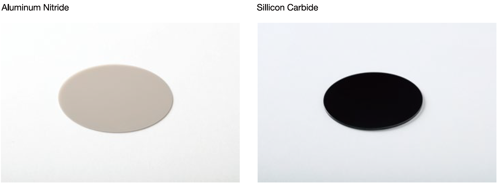
Our NAPHIA™ ceramic wafers are appropriate for semiconductor processes, thanks to the processing technology we have developed through our extensive experience with sapphire wafer polishing. We are able to process any material with minimal damage or grain boundary fractures on the wafer surface, and to a high degree of flatness.
Furthermore, we can do hole processing and cutting of ceramic wafers.

Ceramic wafers
Material SiC (Poly crystal)
Polishing CMP Mechanical polishing
Surface Roughness Ra AFM 0.45nm 0.12nm
P-V AFM 5.75nm 0.97nm
Shape P-V(SORI) ※F.T 1.73μm 1.65μm

※Flatness Tester

Contact

*If you cannot find the contact form, please click here.

☎

Mon-Fri 9:00-17:00 JST+81-3-3919-2200

✉

Online Contact