Direct Exposure Systems (DI Exposure Systems) Features, core technologies, and latest trends
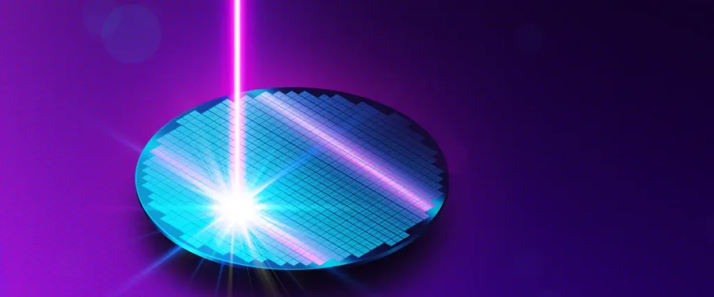
In semiconductor manufacturing, the performance of the final product depends on the accuracy of pattern formation during processing. Exposure technology is an integral part of this process.
In recent years, attention has increasingly focused on direct exposure systems, also called direct imaging (DI) systems, which allow semiconductor circuit patterns to be printed directly onto the substrate without the use of photomasks. As photomask costs continue to rise and demand grows for high-mix, short-cycle production, the ability of direct exposure systems to support flexible design changes has become highly valued.
This article provides a clear and structured overview of direct exposure systems, covering their operating principles, key features, ideal applications, recent trends, and the core technologies that make these systems possible.
Table of contents [close]
What Are Direct Exposure Systems?
Direct exposure systems (DI exposure systems) are exposure tools that print semiconductor circuit patterns directly onto substrates without the need for photomasks. Laser or UV light is used to irradiate the resist layer directly using the design data.
These systems are mainly used in applications where flexibility and speed are required, such as semiconductor prototyping and high-mix, low-volume production. In recent years, their use has expanded to areas including packaging substrates, printed circuit boards (PCBs), and micro-electro-mechanical systems (MEMS).
By eliminating the need for photomasks, direct exposure systems can reduce both costs and development time. Moreover, this approach places greater demands on the underlying exposure and control technologies.
In conventional mask-based exposure systems, such as steppers, pattern transfer is performed by aligning a photomask with the wafer and exposing them together. In contrast, direct exposure systems do not use a photomask. As a result, they require alignment technologies capable of very precise alignment that can accurately detect the wafer position and minutely correct the position during exposure.
Characteristics of Direct Exposure Systems
Some key characteristics of direct exposure systems are:
- No photomask is required.
- Distortion correction can be performed.
- Throughput is generally lower than for other exposure methods.
1. No photomask
Direct exposure systems form patterns by exposing them directly onto the substrate. Therefore, the photomask is not needed.
In conventional photolithography, a photomask is used to transfer the circuit pattern onto the substrate. Direct exposure systems expose patterns exactly as defined in the design data using lasers. This obviates the time, effort, and costs associated with photomask fabrication, management, and storage.
In addition, exposure patterns can be modified by simply updating the design data, allowing rapid response to specification changes. This makes direct exposure particularly effective for applications such as prototyping and low-volume production, where flexibility and turnaround time are critical.
2. Distortion correction
Direct exposure systems can correct the exposed pattern based on the position and shape of the substrate during the exposure process. Rather than simply projecting the design data directly, they enable stable, high-quality pattern formation by accounting for the actual condition of the substrate.
Even tiny distortions on a single substrate can accumulate over multiple exposures and lead to overlay errors and wiring misalignment. By correcting for these during the exposure, direct exposure systems help improve alignment accuracy and enhance the overall quality of the chip.
3. Lower throughput
Direct exposure systems write circuit patterns onto the substrate using laser scanning, partial projection with micromirror devices, or other methods. These methods do not expose the entire substrate all at once. The substrate is divided into multiple regions and exposed sequentially. This tends to increase processing time.
As a result, throughput is generally lower than for exposure methods that process many substrates simultaneously, making direct exposure less suitable for mass production. However, in recent years, advances in techniques such as multi-beam configurations and high-speed systems based on digital micromirror devices (DMD) have increased production speeds.
Ideal Applications for Direct Exposure Systems

Features such as elimination of photomasks and easy modification of design data make direct exposure systems well suited for the following applications:
- Prototyping
- High-mix, low-volume production
- Creating chips on short notice
1. Prototyping
During prototyping, design changes occur frequently. Direct exposure allows pattern modifications to be reflected immediately. By simply updating the design data, changes can be applied directly to the new exposure, eliminating the need to create a new photomask each time the design is revised.
As a result, direct exposure systems help shorten development cycles by enabling fast verification while responding flexibly to design and specification changes.
2. High-mix, low-volume production
Direct exposure systems form patterns without using a photomask, which eliminates the need to create a separate photomask for each product and manage them. Because there are no photomask fabrication costs, creating many different patterns that are used only a few times becomes more feasible.
3. Creating chips on short notice
Direct exposure systems enable chips to be produced more quickly than conventional mask-based exposure methods.
With mask exposure, time is required not only for pattern design but also for photomask fabrication.
In contrast, direct exposure allows exposure to begin as soon as the design data is finalized.
By eliminating photomask creation, direct exposure systems reduce the overall time required for chip creation.
Latest Trends in Direct Exposure Systems
In recent years, direct exposure systems have been gaining acceptance both technically and commercially.
From a technological perspective, advances in exposure methods have led to the development of equipment capable of creating fine patterns of approximately 1 µm, and in some cases as fine as around 0.5 µm. As a result, maskless exposure, previously used mainly for prototyping, can now be used in a broader range of applications, including production. In addition, with the advancement of chiplet integration, which improves performance by connecting multiple chips, the ability of direct exposure systems to correct substrate distortion and misalignment has become a valuable tool.
From a market perspective, the rise of photomask costs is driving adoption of direct exposure systems. As device miniaturization advances, photomask manufacturing costs also increase. This burden is especially acute for manufacturers with diverse product portfolios and therefore a large library of expensive photo masks to manage. In this context, direct exposure systems, which do not require photomasks, are increasingly recognized as an effective means of cost reduction.
By delivering technological advances that improve precision while contributing to lower manufacturing costs and greater efficiency, direct exposure systems are attracting attention and gaining acceptance across a wide range of applications, from research and development to full-scale production.
Technologies Used in Direct Exposure Systems
Direct exposure systems are built on the following core technologies:
- Digital exposure technology
- Positioning and alignment control
- Source light and illumination control
1. Digital exposure technology
Digital exposure technology converts design data into a light pattern that is then projected directly onto the substrate. The pattern is formed using a light modulation device such as a digital micromirror device (DMD).
This enables accurate exposure without the use of a photomask. Because the design data is handled digitally, pattern changes and complex shapes can be accommodated quickly and precisely.
2. Positioning and alignment control
Direct exposure systems require advanced positioning and alignment control because alignment through overlaying a photomask and substrate is not possible.
Substrate position is measured using high-resolution cameras or position-detection sensors, while stage movement is controlled using devices such as laser interferometers or encoders. The acquired positional information is then used to correct distortion and misalignment during exposure.
3. Source light and illumination control
In direct exposure systems, light source intensity, illumination distribution, and focal position is directly linked to exposure accuracy. Optical systems are used to precisely control light output and suppress illumination inconsistencies. Additional key elements include focus adjustment mechanisms based on substrate surface height, and feedback control systems that maintain a constant exposure level.
For these light source and illumination control systems, Orbray utilizes its optical connection technologies, including optical connectors, fiber assemblies, and laser diode modules, to manufacture laser-diode-mounted units for exposure equipment.
In addition, Orbray provides optical design and optical simulation services, enabling integrated support from system design through implementation and assembly.
Direct exposure equipment integrates a wide range of advanced technologies
With its ability to perform complex exposures without using a photomask, direct exposure equipment is highly effective for applications such as prototyping and high-mix, low-volume production. Advanced technologies such as digital exposure and high-precision alignment control are essential for these processes. In addition, the range of applications continues to expand through advances such as pattern-correction functions that compensate for substrate distortion, and support for drawing at the 1-µm scale.
As photomask costs continue to rise, device miniaturization progresses, and optical technologies become increasingly sophisticated, direct exposure is expected to expand beyond research and development into full-scale production environments, offering a balance of flexibility, performance, and cost reduction.
-
Method for mass production of 2-inch diamond wafers developed - Expected to spur industrialization of power-semiconductor devices
と4mm角のダイヤモンド結晶(左).jpg)
-
Surface polishing technologies - Essential technologies for semiconductor, MEMS, and LED manufacturing
-
Lensed Fibers: Brief introduction to the functions and manufacturing methods

-
Launch of the world's first large12-inch high-quality sapphire wafer

-
Precision Nozzles: Materials, Shapes, and Applications
-
What are Porous Ceramics and how are they different from regular ceramics?

