Ultra-Polishing of Sapphire along the c-Plane

Table of contents [close]
Ultra-Polishing of Sapphire Achieved Atomic Level Polishing of Sapphire Achieved
Sapphire is widely used as a substrate for the epitaxial growth of GaN, a semiconductor used in the production of blue LEDs. Sapphire is used because its lattice constant is similar to that of GaN and it can also withstand the high temperatures required for the epitaxial growth of GaN.
To achieve high quality epitaxial growth of GaN, the surface roughness of the sapphire wafer must be as small as possible. However, sapphire is very hard and is considered a difficult-to-process material. Ultra-polishing to the required level is difficult to achieve on an industrial scale. However, through our proprietary “Cutting, Grinding, and Polishing” technologies based on precision industrial jewel processing expertise, Orbray has achieved ultimate sapphire polishing down to the single atomic layer. This precise polishing has led to improvement in epitaxial growth yield of GaN, and has been well received by customers.
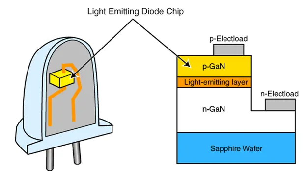
Structure of Blue LED and Characteristics of the Sapphire wafer
The structure of a blue LED is shown below. There is a layer of n-GaN on the sapphire wafer followed by a light-emitting layer, and a p-GaN layer. Electrodes are attached to the p-GaN and n-GaN layers. To increase emission efficiency, the current applied to the light-emitting layer must be uniform. For this, it is important that the underlying n-GaN layer have a uniform crystal structure over the entire surface.
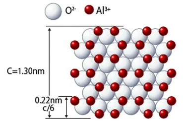
The sapphire crystal is arranged in a hexagonal close-packed structure, with six atomic layers along the c-axis (see the figure below). Therefore, each layer is 0.22 nm thick.
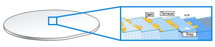
In order to grow a uniform epitaxial layer of GaN across the entire surface, the surface of the sapphire substrate is tilted slightly along the c-plane. If the sapphire is ideally polished, steps will be formed on its surface, as shown in the figure below. GaN is grown in the vapor phase. GaN growth nuclei form at the base of each step and propagate horizontally, creating additional nucleation sites as the crystal grows. This process repeats itself and since the thickness of the step (0.22 nm) is similar to the GaN layer thickness, GaN can grow uniformly over the entire surface of the substrate.
Ultimate Sapphire Polishing
To obtain the ideal sapphire surface, Orbray employs mechanical polishing using abrasive diamond grains to polish the surface, followed by Chemical Mechanical Polishing (CMP). In CMP, mechanical polishing is applied while the sapphire surface is softened chemically. The figure below shows the resulting surface roughness of the sapphire surface using an atomic force microscope.
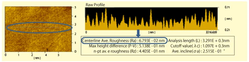
Centerline average roughness (Ra) is approximately 0.06 nm.
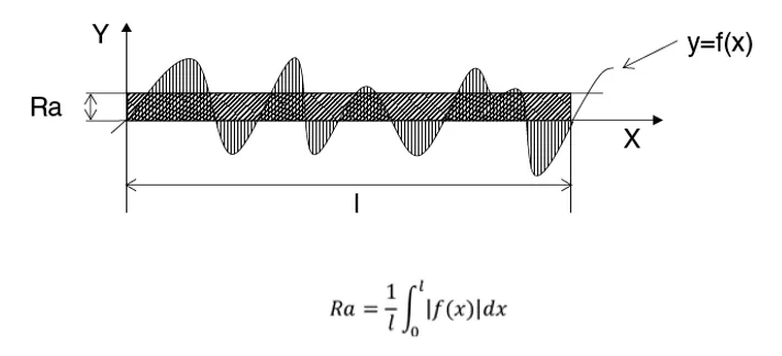
According to JIS “Ra is obtained from the formula shown below when the roughness curve is expressed by y = f(x), taking X-axis to mean line direction and Y-axis to the vertical magnification of the roughness curve in the range of sample reference length l”
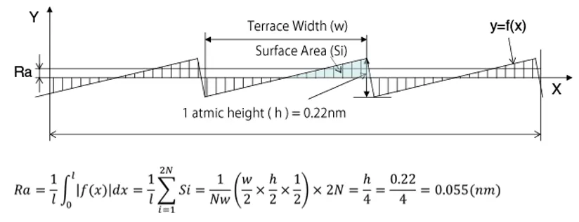
When considering the sapphire surface, the theoretical Ra value when one atomic layer is polished to achieve the ideal terraced structure is calculated as shown below (where h is height, w is terrace width, N is the number of steps, and Si is surface area of the triangle).
Step Substrate
As can be seen, the theoretical Ra closely matches the measured Ra≒0.06 nm. This is evidence that removal of a single atomic layer of the sapphire surface has been achieved. The one atomic layer thick steps and terraces become even more obvious after heat treatment of the substrate. This is called a step substrate.
Since each step has a height of one atomic layer, if the c-plane is offset by 0.15 degrees, theoretically the terrace width is 80 nm. With a height of 0.22 nm and width of 80 nm, this configuration is expected to have many nanoscale applications.
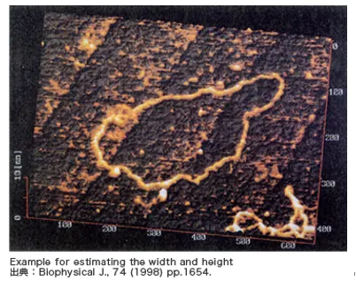
For example, currently, there are no objects to reliably serve as a reference to show scale when imaging nano-sized objects such as DNA. The unique characteristics of the sapphire step substrate can provide a consistent and reliable standard/guide in the nano-world.
In addition, since our sapphire step substrate has an ultra-flat surface, applications related to biological sample analysis, plate nanowires and many other applications are anticipated.
In addition to sapphire, Orbray is able to perform near-ideal polishing of many monocrystal substances suitable for epitaxial growth of compound semiconductors, superconductors, dielectrics, and other applications. Please feel free to contact us about these and other technologies provided by Orbray.


-
Color of Jewel
-
Power semiconductor for EVs: What are they and what are they used for?

-
Method for mass production of 2-inch diamond wafers developed - Expected to spur industrialization of power-semiconductor devices
と4mm角のダイヤモンド結晶(左).jpg)
-
Industrial applications of sapphire
-
World's First Artificial Diamond Substrate Exposure Experiment in Space
-
Introduction to Power Semiconductors: From the basics to applications for each material