Success in mass production technology for ultra-high-purity 2-inch diamond wafer; expected to spur realization of quantum computing

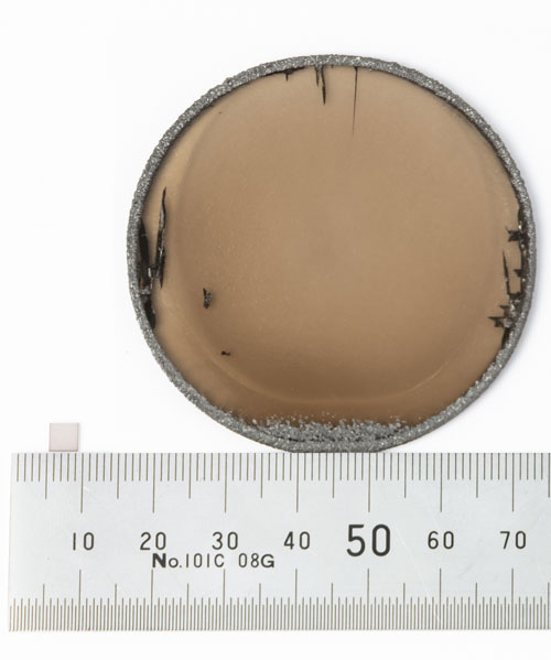
Adamant Namiki Precision Jewel Co., Ltd. (Adachi-ku Tokyo; President and CEO Riyako Namiki) has succeeded in developing a mass production method for ultra-high-purity 2-inch diamond wafers. This ultra-high-purity diamond contains no more than 3 ppb (parts per billion) of nitrogen atoms, as required for quantum applications, such as quantum computers*1, quantum memory*2, and quantum sensing devices. The newly developed diamond wafer has a 2-inch diameter (approximately 55 mm), much larger than the 4mm×4mm crystal currently available. This new technology is expected to propel the advancement of quantum applications. Adamant Namiki plans to commercialize the product in 2023.
On September 9th , 2021, Adamant Namiki Precision Jewel Co., Ltd., in collaboration with Saga University, succeeded in producing a 2-inch diameter wafer (tradename: KENZAN DiamondTM) using a unique step flow method*3. However, that method utilized nitrogen gas to achieve a high growth rate suitable for mass production, but left several ppm (parts per million) of nitrogen impurities, which would affect quantum applications. Since then, Adamant Namiki has improved its production method to achieve its ultra-high-purity 2-inch diamond with no more than 3 ppb of nitrogen, making it appropriate for quantum applications.
By contrast, commercially available ultra-high-purity diamond wafers that contain no more than 3 ppb of nitrogen are only 4mm×4mm. While this wafer size could be used for basic research, it is too small for practical applications. Adamant Namiki has developed a new mass production technology for 2-inch diamond wafers that nearly eliminates nitrogen contamination during the crystal growth process, resulting in ultra-high-purity. A 2-inch diamond wafer theoretically enables enough quantum memory to record 1 billion Blu-ray discs. This is equivalent to all the mobile data distributed in the world in one day.

Adamant Namiki plans to develop peripheral technology, including polishing technology, in preparation for commercial release in 2023. This should greatly accelerate research into quantum devices using large-diameter diamond wafers.
Announcement of research results:
International Conference on Compound Semiconductor Manufacturing Technology 2022
May 10th, 2022
“Two-Inch High-Quality Diamond Heteroepitaxial Growth on Sapphire for Power Devices”
Glossary of terms
*1 Quantum computer
A conventional computer calculates using 2 digits, “0” and “1”. By contrast, a quantum computer would utilize the principals of quantum mechanics. A quantum computer would dramatically shorten calculation time compared to a conventional computer, allowing major breakthroughs in many fields. Competition for development is thus accelerating around the world.
*2 Quantum memory
A type of memory for quantum computers. A diamond crystal defect called NV-center shows high performance for quantum memory in principle. The NV-center consists of a nitrogen atom and a corresponding vacancy in the diamond lattice. This NV-center could form a minute magnetic force and work as quantum memory at the atomic level. Although research is being carried out worldwide using 4mm square diamond crystals, it is difficult to realize practical applications without larger wafers.
In addition to diamond, it is possible to achieve electron spin in other materials as well, but the direction of their spin cannot be stabilized at room temperature. Apparently, only diamond can achieve electron spin at room temperature that is reliable enough for industrial applications, such as in magnetic sensors with both high space resonance and high sensitivity, quantum computing, and bio-marker sensors. For applications that require high resolution and high sensitivity, a diamond crystal with few impurities is necessary, such as the 2-inch diamond that has just been developed by Adamant Namiki.
*3 Step flow growth method
Tilting the crystal orientation of the sapphire substrate by several degrees in relation to the A-plane allows creation of a stepped structure at the atomic level for diamond growth. The crystal grows (flows) in a lateral direction across the steps, greatly reducing heteroepitaxial stress and improving the quality of the crystal. (https://orbray.com/magazine_en/archives/811)
For more information, please contact:
Adamant Namiki Precision Jewel Co., Ltd. Public Relations Office
TEL:+81-3-3919-0101
Saga University Public Relations Division
TEL:+81-952-28-8153
Related Articles:
Method for mass production of 2-inch diamond wafers developed – Expected to spur industrialization of power-semiconductor devices
Novel Diamond Semiconductors Operate at Highest Power Ever
World’s First Artificial Diamond Substrate Exposure Experiment in Space
-
Ultra-Polishing of Sapphire along the c-Plane

-
What are Diamonds?: Synthesis of Diamonds

-
First round of Space Delivery Project “RETURN to EARTH” The ceremony celebrating the return of the payload items was held

-
Launch of the world's first large12-inch high-quality sapphire wafer

-
Introduction to suction nozzles and collets

-
Production of Sapphire


