MEMS technology: Backbone of smartphone and optical communications technology
Tiny electronics components, such as gyrosensors, accelerometers, and optical switches and filters are essential components used in modern electronics, automobiles, and optical communications systems. These components are made using MEMS technology. MEMS is short for Micro Electro Mechanical Systems. The demand for MEMS devices is growing due to the proliferation of smartphones and expansion of IoT applications.
Table of contents [close]
Mechanical and electronic elements in one device
MEMS devices are made by mounting sensors, actuators, switches, and other mechanical elements onto silicon, glass, or organic substrates. They are extremely small, can perform a wide variety of functions, and are highly energy efficient. They are essential for devices that require miniaturization and energy efficiency while maintaining high functionality and precision, such as smartphones, IoT devices, and optical communications devices. Similar to semiconductor devices, MEMS devices can be mass produced, helping to keep costs low.
Unlike semiconductor devices, MEMS devices are structures only several microns in size, often with mechanically moving elements. These devices are mounted on substrates that are a few millimeters in size. These devices make it possible to switch signals on and off; detect acceleration, gravity, and pressure; and manipulate objects that are nano or micrometer in size.
MEMS devices are sometimes called micromachines. However, although there is no set definition, a common distinction is that micromachine refers to tiny mechanical devices with built-in electronic control components, while MEMS refers to devices that combine mechanical, electronic, optical, or chemical elements to achieve some desired function.
How MEMS devices are made
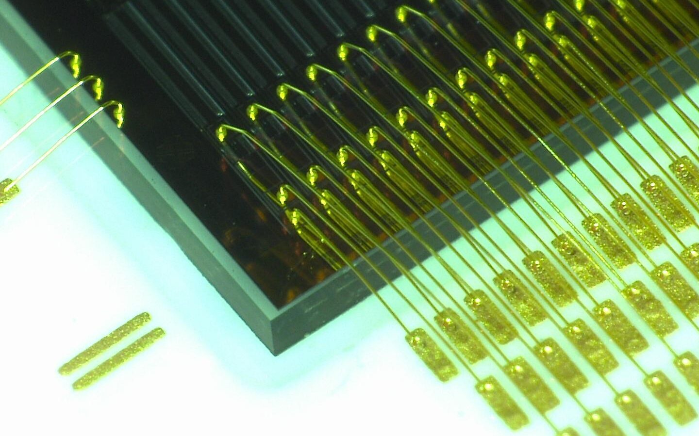
Microfabrication technologies such as semiconductor manufacturing and laser machining methods are used to make MEMS devices. When semiconductor processes are used, resist coating, photolithography, etching, and CVD (chemical vapor deposition) processes are repeated to create the MEMS device on a silicon wafer. The wafer is diced, bonded, and packaged to complete the MEMS device.
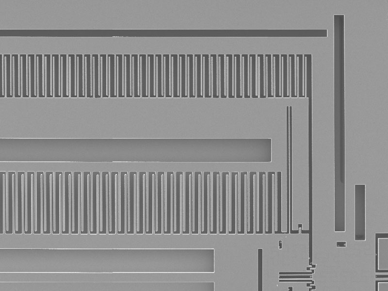
There are two types of etching processes: wet etching and dry etching. If the etching progresses in a single direction, it is called anisotropic etching. If it progresses in multiple directions, it is called isotropic etching. Anisotropic etching uses reactive ions such as fluorine and chlorine to etch deep, straight holes and trenches into the substrate (deep reactive-ion etching, or DRIE). It can be used to etch tiny gears and other features into the surface of wafers.
Sacrificial layer etching is used to create 3-dimensional forms such as levers and hollow shapes. Photolithography and etching processes are repeated to create a sacrificial layer of silicon dioxide on the substrate. This acts as the scaffolding on which to build the target structure. Once the target structure is fully formed, isotropic etching is used to etch away the silicon dioxide layer, leaving only the target structure.
A silicon wafer with structures etched on its surface can be laminated with another wafer that has cavities dug out to accommodate the structures. This creates an airtight seal and is used in the manufacture of MEMS accelerometers and gyroscopes.
MEMS devices in action
MEMS are found in many devices. They have also found applications in chemistry and biology in recent years.
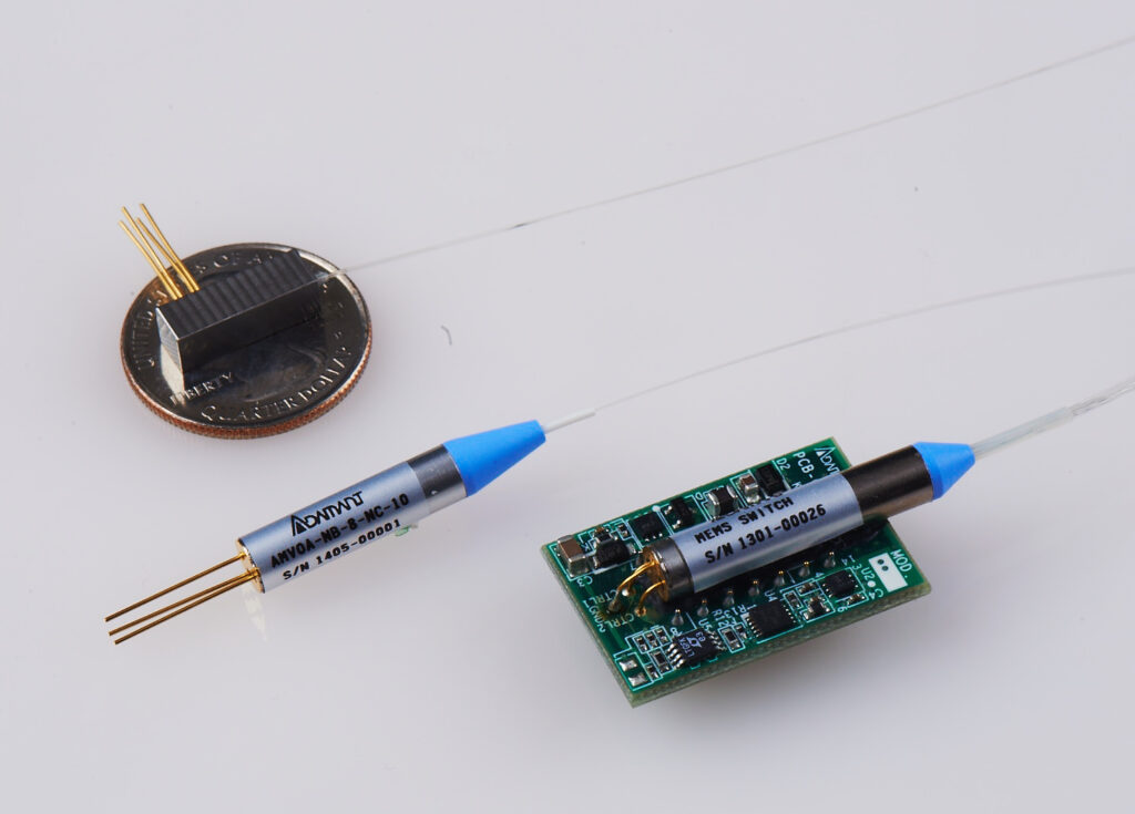
For example, accelerometers, gyrosensors, BAW (bulk acoustic wave) filters, microphones, and other devices made using MEMS technology can all be found in a smartphone. MEMS devices are essential for devices such as smartphones that need to be thin, lightweight, and energy efficient. Cars also use many MEMS devices, such as accelerometers, gyrosensors, pressure sensors, impact and vibration sensors, and many others. Digital micromirror devices (DMD) used in DLP (Digital Light Processing) chips in projectors and 3D printers are also made using MEMS techniques. MEMS devices can also be found in the printer heads of inkjet printers and galvanometers of optical scanners.
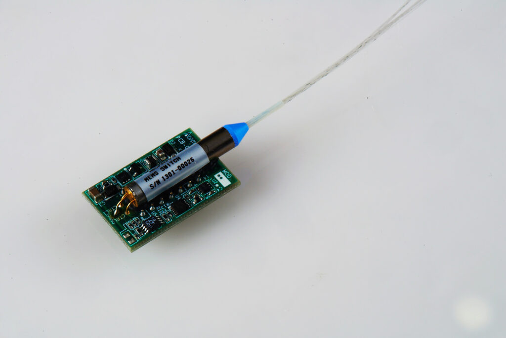
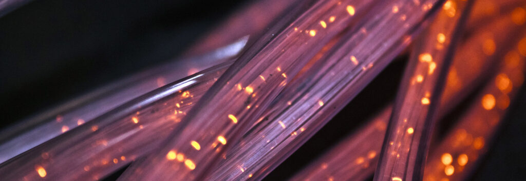
MEMS devices are also being used in optical communications. Optical switches made using MEMS technology are characterized by having low insertion loss, flat wavelength-dependent loss, low polarization-dependent loss, and low crosstalk, enabling high-speed switching in a small package. In addition, variable optical attenuators made using MEMS technology have low insertion loss, wide attenuation range, flat wavelength-dependent loss, and low polarization-dependent loss, and can operate at very low voltage. MEMS devices play an increasingly important role in the development and expansion of optical communications systems.
-
First round of Space Delivery Project “RETURN to EARTH” The ceremony celebrating the return of the payload items was held

-
What is LiDAR? How it works, technologies, and applications

-
High-quality and Large-diameter Diamond Substrates
-
“Physical Contact Push-Pull Technology for Fiber Optic Connectors” recognized as IEEE milestone. Promoting ferrules around the world through manufacturing.
-
Ultra-Polishing of Sapphire along the c-Plane

-
Silicon Photonics: Why is it essential for 5G?