Optical Mounting Technology ( Die bonding / Wire bonding)
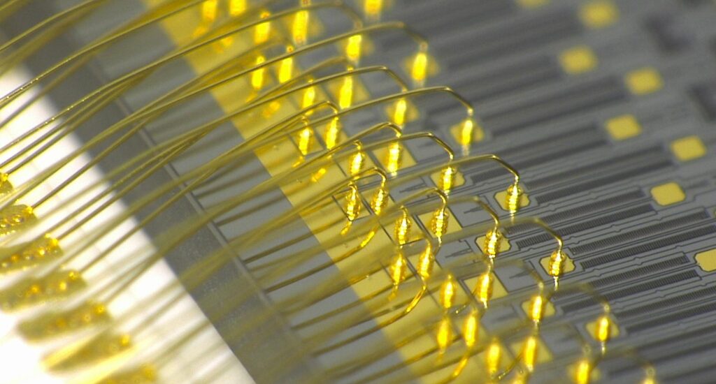
Table of contents [close]
Mounting tiny components for optical, electronic, and MEMS devices
A wide range of electronic and optical components – such as transistors, resistors, integrated circuits, semiconductor lasers, and photodiodes – are used to build advanced electronic devices common in today’s high-tech world. As components become smaller and smaller, the accuracy of their mounting positions becomes even more critical. This is especially true for optical and MEMS components. Advanced mounting technologies and specialized equipment are needed.
Through-hole and surface-mount technologies
The process of attaching individual optical and electronics components to a circuit board is known as mounting. Through-hole technology (THT) and surface-mount technology (SMT) are the two most common mounting methods. In THT, metal leads of each component are threaded through holes in the circuit board and soldered into place. To solder many leads at once, a method called flow-through soldering is used. In this method, all of the components are placed on the circuit board and the leads are cut flush with the underside of the board. Then, the bottom surface of the entire board is covered with a flowing stream of molten solder. This allows solder to be applied to all connection points quickly and uniformly. THT mounting creates strong connections. It also allows for manual addition/removal of components, if needed.
In SMT, the components are soldered to the top surface of the board. A large number of tiny components can be mounted using the SMT method. First, the desired circuit is printed onto the circuit board by using a mask and applying solder over the mask. When the mask is removed, the desired circuit pattern remains on the board. Then, components are placed into the required positions. Because the printed circuits are very fine and the components are very small, high precision is needed when placing the components to ensure that all of the contacts are aligned properly. This task is difficult to do manually, so special equipment such as chip mounters are used. Once all of the components are in place, the entire board is heated in a reflow furnace to melt the solder and complete the connections.
As devices become smaller and thinner, the individual components and their circuits are also becoming smaller. To keep up, mounting technologies must also become more accurate and precise. The miniaturization of THT is limited by the size of the holes and the spacing required between them. Therefore, SMT has become the dominant method as devices have become smaller.
High precision required for optical mounting
Optical mounting refers to the mounting of optical components such as semiconductor lasers, photo-diodes, lenses, optical waveguides, fiber optics, and other optical components. High precision is required for optical components to function properly. Precise optical mounting allows signals from electronic circuits to be converted into optical signals and transmitted. Therefore, it is necessary to create circuits than can connect to electronic components to receive and transmit optical signals.
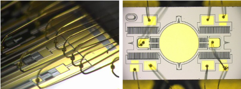
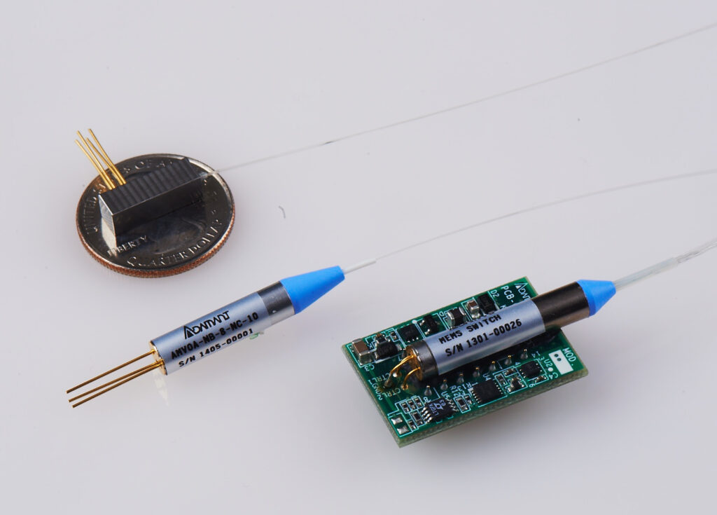
To make the electrical connection to the lead frame, the semiconductors of optical devices such as semiconducting lasers are attached to the case in which the lead frame is incorporated. The chips can be attached in one of two ways. In the die bonding method, adhesives such as solder, silver paste, and UV activated epoxy are applied to the casing.
In the wire bonding method, minute wires made of materials such as gold are used to connect the chips to the lead frame. After bonding, the chip is made airtight and mounted onto the circuit board.
Optical components are becoming ever smaller as the miniaturization of electronics devices progresses. As a result, chips have become more minute, creating a need for increased accuracy and reproducibility in die bonding and mounting.
In addition, compared with the mounting of electronic components, greater care is needed in the mounting of optical components to ensure performance. The slightest misalignment or reflection of light can greatly impair the functionality of the entire device. For optical devices to perform at the required levels, they must be mounted very precisely every time.
Precise placement and high reproducibility are required
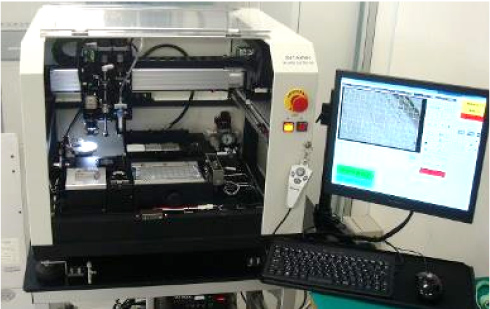
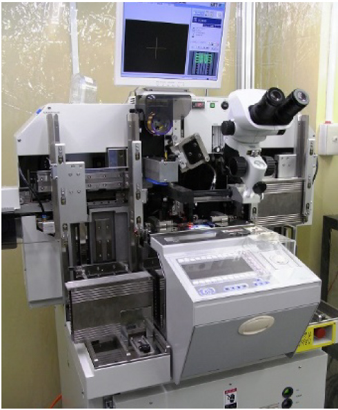
Advanced technologies and specialized equipment are required for mounting tiny optical and electronic components, and devices such as MEMS components. Due to continual advancements in technology, these components are now so small that they are difficult to see with the naked eye. Tiny MEMS devices, such as gyroscopes and microswitches, are being used in a wide range of consumer and high-tech products.
Very accurate placement with high reproducibility is required to mount a large number of such tiny devices close together onto a circuit board. In addition, each piece must be placed onto the board very quickly to ensure adequate throughput of the manufacturing process. Furthermore, very high accuracy is needed when placing and bonding optical components because the optical elements themselves are manufactured with extremely high dimensional precision. Placement must be exact to ensure optimal performance.
-
Silicon Photonics: Why is it essential for 5G?

-
Lensed Fibers: Brief introduction to the functions and manufacturing methods
-
MEMS technology: Backbone of smartphone and optical communications technology
-
Surface polishing technologies - Essential technologies for semiconductor, MEMS, and LED manufacturing
-
Award: Industrial Standardization Enterprise Award

-
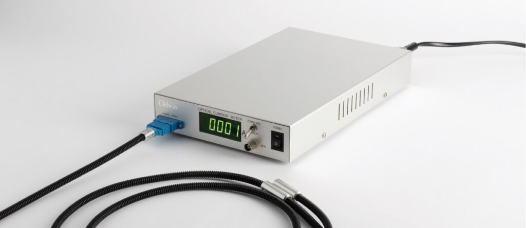
Optical Fiber Current Sensors