Introduction to Power Semiconductors: From the basics to applications for each material

Power semiconductors are semiconductor devices designed to control large amounts of power. Mass production of high-quality power semiconductor materials became feasible recently. This has led to the widespread use of these semiconductors in various fields, including electric vehicles (EVs), smart grids, and renewable energy sources.
In this article, we will describe what power semiconductors are, discuss the unique characteristics of each material, and explore the various fields where they are being applied.
Table of contents [close]
Features of Power Semiconductors
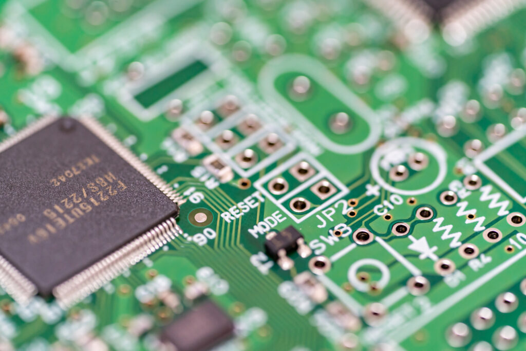
Semiconductors are used in many electronic devices that surround us in our daily lives.
For example, they are used in solar panels, where semiconductors are the main material. These semiconductors take advantage of a unique characteristic: electrons in them become mobile upon exposure to light. In contrast, LEDs, commonly used in displays and lighting, operate in the opposite way. They transform electric current into light, showcasing another versatile use of semiconductors.
Current Control
One very important function of semiconductors is “current control.” This involves regulating the flow of specific types of electricity. This is vital in a wide range of applications, such as computers, home appliances, and light switches.
For example, a semiconductor device known as a diode permits current to flow only in one direction and blocks it in the opposite direction. Another device, the transistor, functions like a gate, controlling the ON/OFF states of current.
The logic circuits inside computers are built by integrating these switching devices.
AD Conversion
Electric power is transmitted through wires as alternating current (AC) to minimize power losses during transmission. However, most household appliances run on direct current (DC). Therefore, AC must be converted to DC for practical use.
Diodes are employed in this AC to DC conversion process, also known as AD conversion. Below is a diagram illustrating the current waveform in AD conversion using a diode.

When alternating current passes through a diode, it blocks the current flowing in the opposite direction (the lower half of the waveform in the diagram), leaving only the upper half. If another device is used to shape the waveform, the DC current is completed. In actual AD conversion, efforts are made to utilize the otherwise wasted cut-off lower half.
However, if the signal frequency (how often the current direction changes per second) increases, the device may struggle to keep up, leading to waveform distortion and increased power loss during the conversion to DC.
Before semiconductors, AD conversion was performed with non-semiconducting devices, but these methods resulted in significant power loss and inefficiency.
Thanks to their fast switching speeds, semiconductors minimize power loss during AD conversion, making the process more efficient.
What are Power Semiconductors?
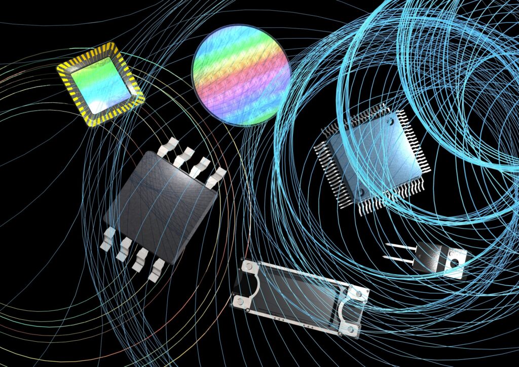
Silicon-based semiconductor converters work well for AD conversion in general household appliances. However, for applications such electric vehicles (EVs) and Shinkansen (bullet) trains, the requirements are much different.
Semiconductor devices have a maximum voltage threshold; exceeding this can lead to dielectric breakdown, damaging the device. Power semiconductors were developed to address this issue. Power semiconductors are devices that are capable of efficient switching without dielectric breakdown, even under high voltage conditions.
The term “power semiconductor” refers to a specific category within semiconductor devices. The key distinction between regular semiconductors and power semiconductors lies in their usage.
While increasing the size of a silicon device can enhance its resistance to dielectric breakdown, there are reasons why large silicon power devices are not typically used.
Requirements of Power Semiconductors
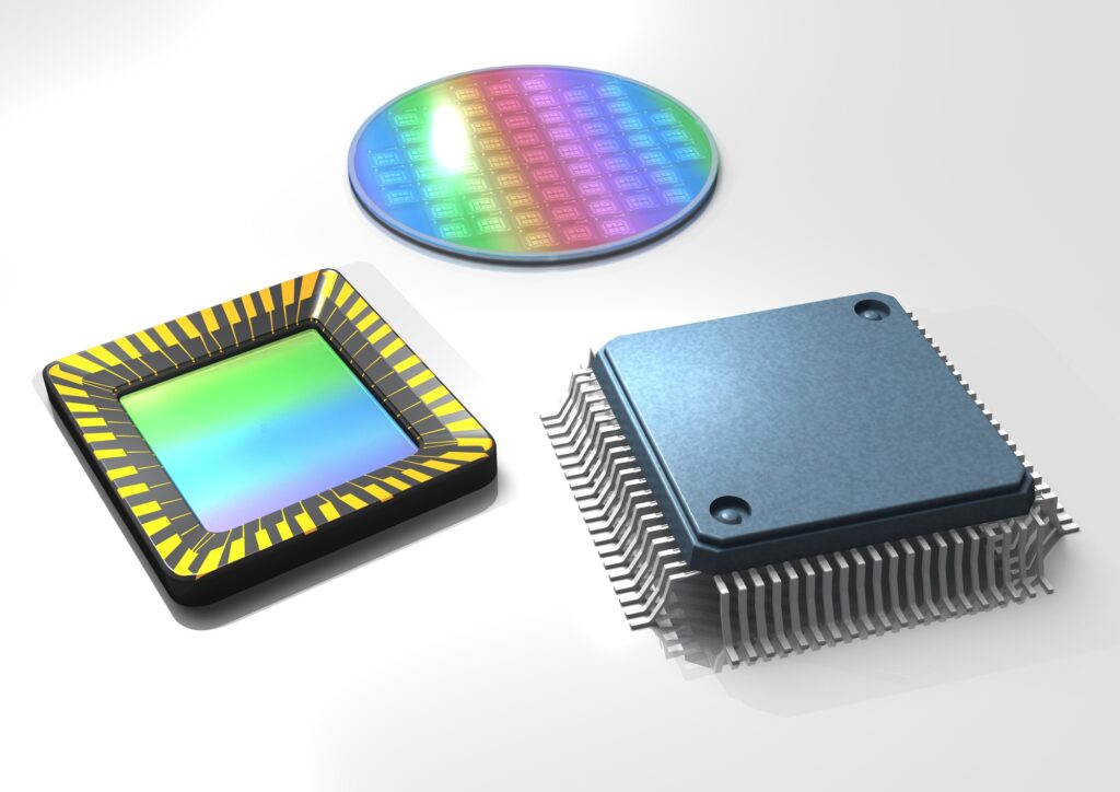
Characteristics desired from power semiconductors can be summarized as follows:
・High dielectric breakdown voltage
・High switching speed
・Cost effectiveness and high production capacity
・High heat resistance.
As mentioned, even a single silicon device can serve as a power semiconductor. However, creating a large silicon power device presents challenges: it would occupy considerable space, which hinders practical use, and its switching speed would be reduced. Consequently, material improvements are crucial to achieve both high resistance to breakdown and low power loss.
The question then arises: how can we enhance both the dielectric breakdown voltage and the switching speed of power semiconductors?
Dielectric breakdown voltage and band gap
One way to increase the dielectric breakdown voltage is to increase the band gap.
Band gap refers to the energy range in a solid material where no electronic states exist. The larger the band gap, the less likely dielectric breakdown is to occur.
To simplify this complex idea, let's compare the band gap to a dam.
Imagine a dam positioned between an upstream and a downstream reservoir. The upstream reservoir, or the valence band, is filled with water representing electrons. The dam, equating to the band gap, separates this from the downstream area, known as the conduction band, where electrons can move freely. Normally, the dam prevents water (electrons) from flowing downstream.
If the upstream water pressure becomes too strong for the dam to hold back, it will burst, allowing water to flow downstream freely.
Similarly, when a high voltage (analogous to high water pressure) is applied, it can force electricity across the band gap (akin to breaking the dam), leading to what's known as dielectric breakdown.
The band gap value is determined using a theoretical formula. The closer the atoms in a semiconductor are to each other, the larger the band gap, and consequently, the higher the dielectric breakdown voltage.
Switching Speed and Mobility
The switching speed of a semiconductor is related to how fast electrons can move within the semiconductor. This is known as mobility.
Although the theoretical value of mobility can be calculated from the material property of the crystal, it changes depending on factors such as the density of impurities and lattice defects, as well as the state of the semiconductor surface, so it is not possible to attain the theoretical value. In order to create devices with high mobility, it is important not only to select proper materials, but also to create high-quality crystals and combine them with other materials.
Characteristics of various power semiconductor materials and applications
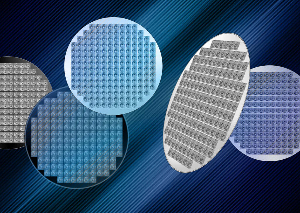
SiC, GaN, and diamond are materials that have both large band gaps and high mobility, making them ideal for use in power semiconductor devices.
| Silicon | SiC | GaN | Diamond | |
| Band gap | 1 | 3.3 | 3.4 | 5.5 |
| Dielectric breakdown strength | 1 | 9.3 | 8.3 | 33 |
SiC power semiconductors have reached a stage where they are now starting to find practical application. Many institutions began R&D with SiC early in development. Now, mass production systems are starting to crop up one after another.
For example, Tesla, a leading EV manufacturing company, has incorporated SiC in its electric vehicles, particularly in the power control systems related to charging (*1). Following Tesla's lead, major SiC device manufacturers are now increasingly collaborating with EV producers (*2-4).
In comparison, GaN power devices are more expensive than SiC ones, but their performance, especially in terms of mobility, is nearly double that of SiC devices.
Diamond power semiconductors, currently in the research stage, are gaining interest. They exhibit excellent voltage resistance and switching capabilities, and remain stable in high-temperature and radiation conditions, making them ideal for power semiconductor applications.
Various applications, such as use in communications satellites, are being considered.
The future of diamond semiconductors

In this article, we explored the characteristics of semiconductors and power semiconductors. Although diamond semiconductors are still in the research stage, their high performance compared to other materials is attracting attention in a wide range of fields, from EVs and power conditioners, to next-generation communications, medical care, nuclear power, space, and robotics.
We will further explore diamond semiconductors in a future article.
-
Industrial applications of sapphire

-
Summary of “Grinding” and “Polishing”A brief introduction to these processing technologies and how they are used.

-
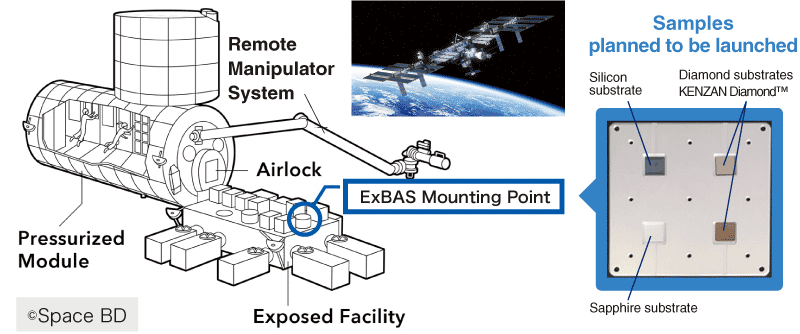
World's First Artificial Diamond Substrate Exposure Experiment in Space
-
TIME Asia interviewed President Riyako Namiki

-
Jewel bearings: Orbray and the watch industry [Story of Watch 1]

-
Diamond Wafers: Production Technologies and Applications
