We were featured on the cover of the journal Diamond and Related Materials.
Through collaborative research with Korean Polytechnical University (KPU), Schottky Barrier Diodes were created on synthetic diamond substrate (KENZAN Diamond®) grown heteroepitaxially on sapphire substrate. The article details the creation of the Schottky Darrier Diode, and elaborates on the possibilities of practical applications of the process.

With an ideal coefficient of 1.4, SBD with breakdown voltage of 1.1 MV/cm was obtained.
We were featured on the cover of the journal Diamond and Related Materials.
Through collaborative research with Korean Polytechnical University (KPU).
The Diamond Schottky barrier diode (SBD) was successfully fabricated on sapphire-based freestanding heteroepitaxial diamond substrate (KENZAN Diamond®) using Microwave Plasma Chemical Vapour Deposition(MPCVD).
Considering the electrical characteristics of heteroepitaxial SBD, a growth rate of diamond epitaxial layer significantly affects the device performance owing to its surface morphology and crystal quality. The ideality factor of 1.4 and maximum breakdown field of 1.1 MV/cm were achieved by power device analyzer respectively.
Copyright Elsevier

About the journal
DRM is a leading international journal that publishes new fundamental and applied research on all forms of diamond, the integration of diamond with other advanced materials and development of technologies exploiting diamond. The synthesis, characterization and processing of single crystal diamond, polycrystalline films, nanodiamond powders and heterostructures with other advanced materials are encouraged topics for technical and review articles.

Table of contents [close]
- 1. Diamond Schottky barrier diodes fabricated on sapphire-based freestanding heteroepitaxial diamond substrate
- 1.1. 1. Introduction
- 1.2. 2. Experimental
- 1.3. 3. Result and discussion
Diamond Schottky barrier diodes fabricated on sapphire-based freestanding heteroepitaxial diamond substrate
Taemyung Kwak (a), Jonggun Lee (a), Uiho Choi (a), Byeongchan So (a), Geunho Yoo (a), Seongwoo Kim (b), Okhyun Nam (a)
(a) Convergence Center for Advanced Nano Semiconductor, Department of Nano-Optical Engineering, Korea Polytechnic University, Siheung 429-793, Republic of Korea
(b) Adamant Namiki Precision Jewel Co., Ltd., Tokyo 123-8511, Japan
ABSTRACT
In this study, diamond Schottky barrier diodes (SBDs) fabricated on a sapphire-based heteroepitaxial diamond substrate were demonstrated. For commercializing diamond-based power electronics, a large-sized heteroepitaxial diamond substrate is essential. Sapphire is one of the most promising candidates among the diamond heteroepitaxial substrates because it can be produced on a large scale and its thermal expansion coefficient is similar to that of diamond, compared to that of any other non-diamond hetero substrate. The current-voltage characteristics of heteroepitaxial diamond SBDs grown under different growth rates were analyzed, and good rectification properties of SBDs were observed at the device grown with low growth rate. The ideality factor was 1.4, and the maximum breakdown field was approximately 1.1 MV/cm. The value of built-in potential derived from the capacitance-voltage characteristics was in good agreement with the approximated barrier heights. Some
ball-shaped features on the SBD along the threading dislocation were directly observed after performing the breakdown test under reverse bias condition using transmission electron microscope (TEM). Threading dislocation which induces breakdown or large leakage current under reverse bias in diamond SBD was clarified and this will lead the research direction of a heteroepitaxial diamond electronic device.
Prime novelty statements: Recently, the diamond SBD grown on large-size heteroepitaxial diamond substrates becoming alternative to conventional high temperature high pressure (HPHT) diamond-based diamond SBD. In this study, diamond SBD grown on sapphire-based freestanding heteroepitaxial diamond substrate was successfully
demonstrated. The sapphire substrate is one of the most promising material as substrate for heteroepitaxial
diamond which is low cost and large sized. The heteroepitaxial diamond SBD structures with different growth rate were grown using microwave plasma CVD (MPCVD) and its structural properties were characterized.
After device fabrication process, the detailed analysis of electrical properties of SBD were carried out. The direct observation of breakdown and leakage current features on SBD was obtained before and after electrical test under reverse bias condition.
1. Introduction
In the field of ultra-wide bandgap semiconductor materials, single crystal diamond semiconductor is considered to be one of the most attracting candidate materials for the next-generation power electronic devices owing to its very high carrier mobility, excellent breakdown field, and thermal conductivity. A diamond semiconductor is expected to be the most appropriate to use in a harsh environment than any other wide-bandgap semiconductor materials. For these reasons, several previous studies of diamond power electronic devices such as Schottky barrier diodes (SBD) and field-effect transistors have been reported [1,2]. The SBD is an essential discrete device as a power circuit component. In particular, diamond-based SBD is considered to be advantageous owing to its low turn-on voltage, fast reverse recovery time, and the possibility of high temperature operation [3–5]. However, diamond has disadvantages such as small size and very high cost. For these reasons, the heteroepitaxy of diamond via microwave plasma chemical vapor deposition (MPCVD) have been studied for a long decade; consequently, a 4-in. sized diamond substrate grown on Ir/Yttria stabilized zirconia/Si was reported [6].

Recently, the heteroepitaxial iamond SBD was grown on large-sized foreign substrates such as Si, MgO and SiC as an attempt to provide a possibility of commercializing diamond-based electronic power devices [7,8]. In this study, a diamond SBD grown on a sapphire-based freestanding heteroepitaxial diamond substrate was demonstrated. Sapphire is considered to be one of the most promising material as substrate for growing heteroepitaxial diamond owing to its low cost and large size. We investigated electrical and structural properties of diamond SBDs grown with different growth rates using a power device analyzer. The breakdown analysis of heteroepitaxial grown diamond SBD has not been reported yet. The position where device breakdown occurred was observed using a TEM.
2. Experimental
2.1. Growth of diamond SBD epilayer
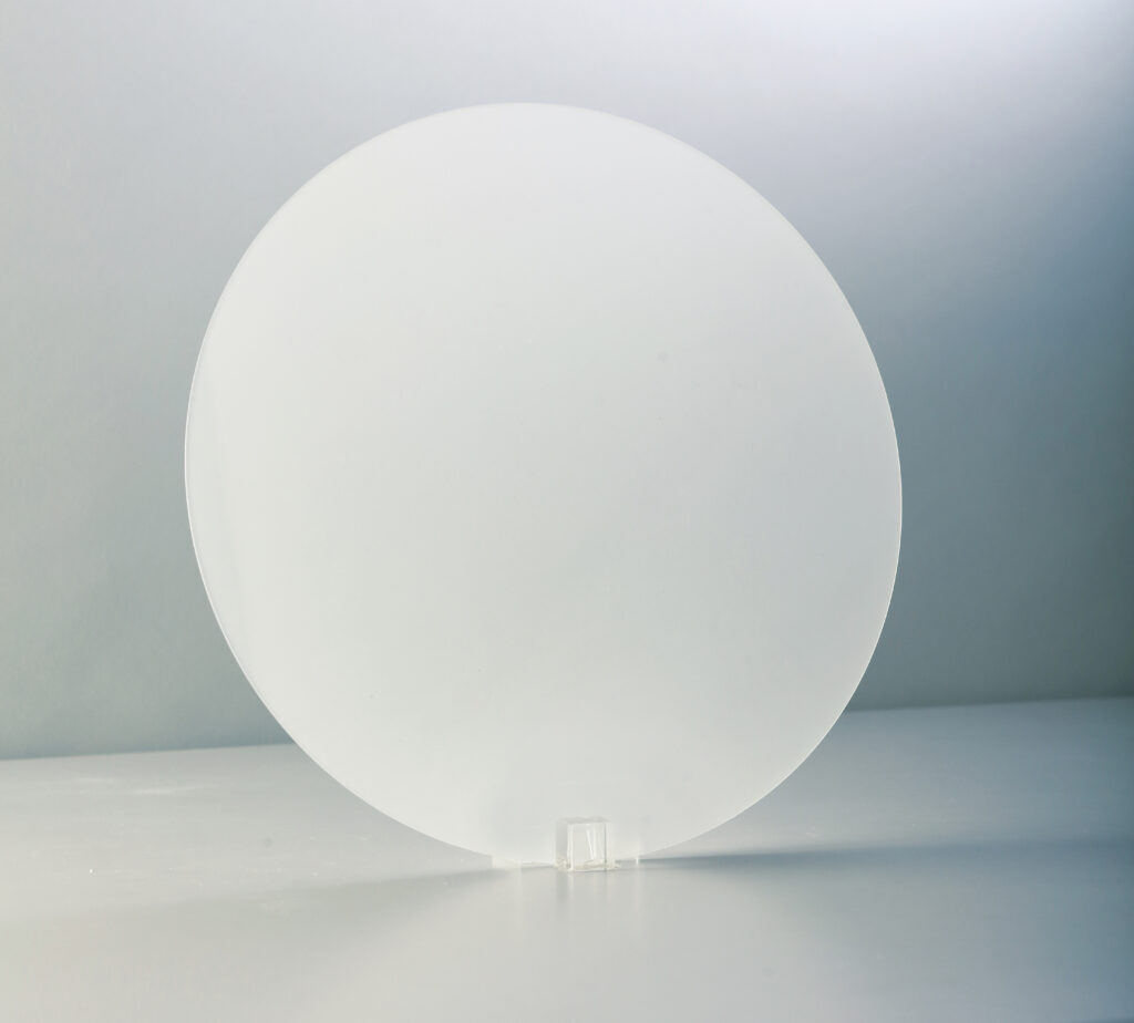
The pseudo-vertical diamond SBD was grown using NIRIM-type MPCVD system. Here, 2.45 GHz of microwave and 1000 W of microwave power were used for growing the epilayer. Two different SBD samples were grown on heteroepitaxial diamond substrates by controlling the CH4/H2 ratio (5% and 1%). In this experiment, we used freestanding heteroepitaxial diamond substrates (8 × 8 mm2) developed by Orbray Precision Jewel Co., Ltd., and they were grown on alphasapphire substrate by applying a stress reduction technique involving a thermochemical reaction between nickel and carbon, which has been described in detail elsewhere [9,10]. The diamond substrate was cut into four pieces and chemically cleaned with acetone, isopropyl alcohol, and deionized water for 10 min during each procedure. The source gas was methane diluted with high-purity H2, and boron doping gas was Triethyl borane (TEB). At first, a heavily boron-doped p+ layer of 1 μm was grown with TEB/CH4 (B/C) in a ratio of 500 ppm for reducing the contact resistance and for spreading current easily. Then, a p- drift layer with a thickness of 1 μm was unintentionally doped while depositing owing to residue inside the reactor. In our previous study, we experimentally obtained the doping range for each p+ and p- layer, and the doping concentrations were 1 × 1020 cm-3 and 1 × 1016 cm-3, respectively [11]. The detailed growth conditions of diamond SBD are listed in Table 1.
2.2. Fabrication process
For fabricating diamond SBD, the as-grown p+/p- SBD epilayer was treated with an acid-mixture of sulfuric acid and nitric acid at 200 ◦C for 30 min for oxidizing the H-terminated diamond surface. The diamond SBD was patterned via photolithography using DNR-300 L negative photoresist, and an aluminum thin film with a thickness of 300 nm was deposited as an etching mask. To isolate a device, etching process was conducted toward the substrate region by considering the process parameters of a gas mixture of O2/Ar with a flow rate of 20/20 sccm and an ICP power of 600 W. The p- /p+
diamond samples with a thickness of 2μm were etched and evaluated using an alpha-step surface profiler.
Thereafter, ohmic contacts were made on the diamond surface by evaporating Ti 50 nm followed by Au 100 nm to prevent the oxidization of Ti electrode. The samples were later annealed at 500℃ for 1 h in argon atmosphere to form TiC alloy. An aluminum Schottky electrode with a diameter of 100 μm and thickness of 100 nm was deposited and patterned via the lift-off process.
2.3. Characterization method
The surface of boron-doped diamond samples was observed using an FE-SEM (Hitachi, S-4000). The double crystal X-ray diffraction measurement system (Panalytical, X’pert pro) and Raman spectroscopy with an excitation source of 532 nm laser (NOST, HEDA) was mainly used to evaluate the crystal quality and stress of the sample. The electrical properties of boron-doped diamond layer was characterized using a high-temperature Hall effect measurement system (Lakeshore, HL5500).
The height of fabricated patterns was profiled using an Alpha-step (D-500, KLA-Tencor). The incorporation of boron was measured using secondary ion mass spectroscopy (SIMS, Cameca, IMS-7f). The O+2 were used as the primary ions and they were accelerated to 10 keV (raster size was 175 × 175 μm2). The boron concentration was quantified using a standard sample.


Before high-resolution TEM analysis, diamond SBD samples of size 10 × 10 × 0.2 μm (W × H × T) were prepared using focused ion-beam (FEI, NOVA nano 600 Fab). The cross-sectional structural analysis of SBD was performed using an HRTEM (JEOL, JE- 2100f) with an acceleration voltage of 200 kV. The device characterization was examined using a power device analyzer (Keysight, B1505A).
3. Result and discussion
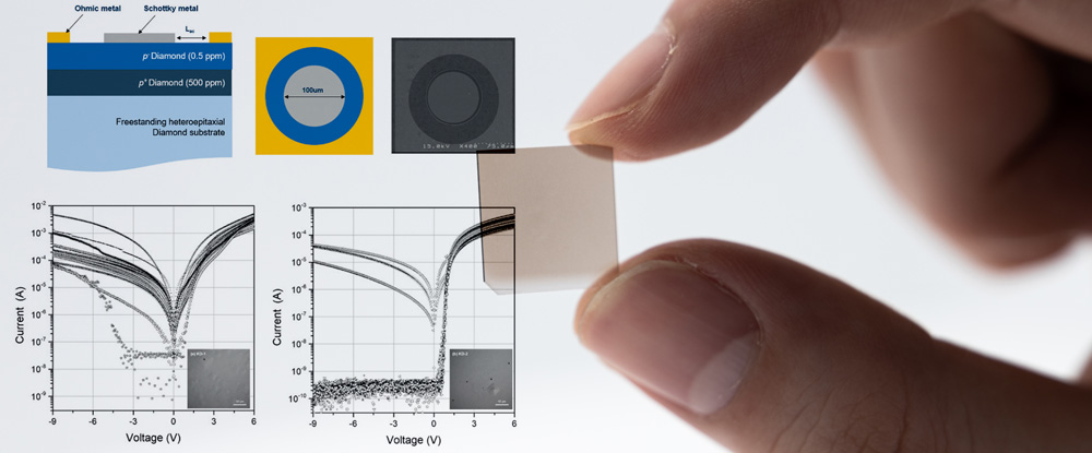
Fig. 1 depicts the cross-sectional and aerial view of the schematic structure of the diamond SBD grown on sapphire-based freestanding heteroepitaxial diamond substrate and its surface image captured using FE-SEM. The design of the device pattern was referred to previous study of diamond SBDs [12]. The length from anode to cathode is 10, 20, 30, 40 and 50 μm, and all of the Schottky metal diameter is 100 μm.

Fig. 2 shows the microscopic image of the as-grown diamond SBD epilayer. Despite the same quality of heteroepitaxial diamond substrate, as the methane flow rate increased, the total amount of surface defect of the diamond SBD such as flat hillock (FH), pyramidal hillock (PH) and non-epitaxial crystal (NC) also increased from 2.4 × 10⁵ to 1.6 × 106 cm-2 and these are depicted in Fig. 2, respectively. The current-voltage (I-V) characteristic result of 15 diodes were measured at 300 K from each diamond SBD (KD-1,2) sample and are depicted in Fig. 3.
Fig. 3(a) indicates poor rectification due to PHs and FHs of the SBD epilayer, which might have generated from the dislocation core of heteroepitaxial diamond substrate during the growth along the growth direction with high methane flow rate. Whereas Fig. 3(b) shows I-V curves of sample KD-2 with an improved on/off ratio of 106 at ±6 V. In particular, when FH or PH was located in the Schottky electrode region among surface defects as shown in inset, I-V curves with step at forward and large leakage current were observed. It is demonstrated that these surface defects originated from 60◦glide type dislocation generated by metal impurities from susceptor were suppressed under low growth rate condition [13].
We observed that the dispersion of current at +6 V was attributed to the difference in the parasitic resistance on p + layer with an increase in the length from anode to cathode (from 10 μm to 50 μm). To evaluate the electrical properties, value of barrier height and ideality factor of SBD sample KD-2 were extracted from forward characteristics as depicted in Fig. 4(a) by using thermionic emission model: [14].

where parameters A*, T, q, ϕb, n, kB, and RS are the Richardson constant (90 A/cm2K2), temperature, electron charge, barrier height, ideality factor, Boltzmann constant, and series resistance, respectively [15]. The electrical characteristic of KD-2 exhibited a barrier height of 0.74 ± 0.03 eV with an ideality factor ranging from 1.6 to 3.0 which is probably due to the rough surface or the inhomogeneity of the O-terminated diamond junction with Schottky metal [16]. Another reason for the wide distribution of ideality factor could be the surface defects of the diamond, such as hillocks or NCs.
Fig. 4(c) depicts the C–V characteristics of diamond SBD (KD-2) measured at 300 K and at a frequency of 5 kHz. The doping uniformity of SBD was almost homogenous, and the net dopant concentration of NAND was 8 × 1015 cm-3 (derived from 1/C2-V curves). The built-in potential of the diamond SBD was approximately 1.1 eV, which is the xaxis intercept of 1/C2-V curves, and this is in good agreement with the zero-bias barrier height of 1.5 eV referred equation for the low-borondoped diamond: [17].

Fig. 5 depicts the reverse bias characteristics of diamond SBD measured from voltage range up to -100 V with high dielectric liquid (Fluorinert, 3 M Inc.) to avoid air breakdown.

Consequently, irreversible electrical breakdown and large leakage current occurred at -50 V, which could be attributed to the threading dislocation. After the breakdown, large level of leakage current flowed through the Schottky and ohmic electrodes. The design of diamond SBD is a punch-through type diode with 1 μm thick and acceptor concentration of 2 × 1016 cm-3 of p-type drift layer. The breakdown field of diamond SBD can be expressed as

where E, Vbi, V, and W are the electric field, built-in potential, applied voltage, and depletion width, respectively [18]. The maximum breakdown field of heteroepitaxial diamond SBD derived from the equation was 1.1 MV/cm, which is considerably less than the theoretical value of the diamond owing to the high dislocation density of the heteroepitaxial diamond epilayer.
Before TEM analysis, the diamond surface at the Schottky electrode region was revealed after removing Aluminum with HCl. Thereafter, defect-related etch pits were formed via H2/O2 plasma treatment for 2h, as shown in Fig. 6.
Consequently, two types of etch pits were observed, which are point bottom and flat bottom shaped pits related to the intrinsic defect of heteroepitaxial grown diamond and polishing damage induced by polishing groove, respectively [19]. After plasma etching, the incorporation of boron impurity in the p+ contact region and p- drift region of KD-2 evaluated using secondary-ion mass spectroscopy (SIMS) as shown in Fig. 7.
To investigate the origin of SBD breakdown or large leakage current, we fabricated a diamond specimen to observe the dislocation of diamond SBD via TEM. Fig. 8 (a) depicts the cross-sectional TEM image of the diamond SBD (KD-2) with a zone axis of [110] plane. Yellow arrows indicate the threading dislocations of the diamond along the [001] direction, and interestingly, some ball-shaped features were observed along the dislocation line, as shown in Fig. 8(b). When doping with a high dopant concentration of 3 × 1021 cm-3, analogous features due to dopant agglomeration have been reported in the literature [20]. The other assumption of these features is structural evidence of electrical breakdown. Note that there are no ball-shaped features as shown in Fig. 8(c) at the spot near the region in Fig. 8(a), which were located out of the device region. Further investigations of these ball-shaped features along the threading dislocation in the diamond epilayer are required.
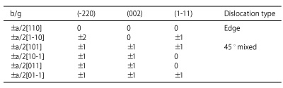
To classify the types of dislocations where breakdown or large leakage current occurred, invisible criteria (g⋅b = 0) were used in TEM.
Dislocations propagating along [001] in the diamond layer were observed with different g-vector. Typically, these [001] dislocations are classified into two types of edge and 45◦mixed type dislocations. The relationship between the burgers vectors of [001] dislocations with gvector in this study was shown in Table 2. Fig. 9 shows a cross-sectional TEM dark-field image of diamond SBD taken in two-beam diffraction conditions of (a) g = 002, (b) g = -220 and (c) g = 1–11 respectively.
Yellow arrows indicating [001] dislocation generated from substrate were shown. All the [001] dislocations in Fig. 9 were identified as 45◦ mixed dislocation propagated from a heteroepitaxial diamond substrate.
Table 2
The combinations of the diffraction vector g, Burgers vector b and its dislocation
type in diamond SBD epilayer.


According to previous study of defects in diamond using X-ray, most of 45◦ mixed dislocation was generated at the interface during homoepitaxial diamond growth due to polishing damage [23]. Furthermore, 45◦ mixed type, rather than edge type, requires less energy to form defects [24]. In the case of heteroepitaxial growth, it seems that there will be a more complex defect generation mechanism due to the stress caused by the lattice constant mismatch between substrate and diamond epilayer [21].
The diamond SBD fabricated on an HPHT diamond substrate was reported a low specific on-resistance with high blocking voltage near the theoretical limit of the diamond. The heteroepitaxial diamond-based SBDs have still low breakdown voltages and high specific onresistance compared to HPHT-based diamond SBD devices. Diamond SBDs fabricated on various types of heteroepitaxial substrate have been reported. The heteroepitaxial Diamond SBD fabricated on Ir/SrTiO3/Si (001) shows breakdown voltage of ~50 V with specific resistance of 150 mΩ∙cm2 and different type of heteroepitaxial diamond SBD grown on Ir/YSZ/Si(001) with high specific on-resistance of 5 Ω∙cm2 was reported [22]. These results still show low breakdown voltage and size limited issues in heteroepitaxial diamond-based devices. To improve device performance, the crystal quality of heteroepitaxial diamond should be improved by annihilation or blocking threading dislocation using defect reduction techniques such as epitaxial lateral overgrowth for diamond on a freestanding heteroepitaxial diamond substrate.
4. Conclusion
In summary, the diamond Schottky barrier diode was successfully fabricated on sapphire-based freestanding heteroepitaxial diamond using MPCVD. Considering the electrical characteristics of heteroepitaxial SBD, a growth rate of diamond epitaxial layer significantly affects the device performance owing to its surface morphology and crystal quality. The ideality factor of 1.4 and maximum breakdown field of 1.1 MV/cm were measured by power device analyzer respectively.
Most of threading dislocations in Diamond SBD epilayer grown on heteroepitaxial diamond substrate revealed as 45◦ mixed type deteriorating the device performance, that induced early breakdown or large leakage current. The results suggest that sapphire-based CVD grown heteroepitaxial diamond substrate can be used for the application of waferscale diamond electronic devices.
Author statement All persons who meet authorship criteria are listed as authors, and all
authors certify that they have participated sufficiently in the work to take public responsibility for the content, including participation in the concept, design, analysis, writing, or revision of the manuscript.
Furthermore, each author certifies that this material or similar material has not been and will not be submitted to or published in any other publication before its appearance in the Diamond Related Materials.
Declaration of competing interest
The authors whose names are listed immediately below certify that they have NO affiliations with or involvement in any organization or entity with any financial interest (such as honoraria; educational grants; participation in speakers’ bureaus; membership, employment, consultancies, stock ownership, or other equity interest; and expert testimony or patent-licensing arrangements), or non-financial interest (such as personal or professional relationships, affiliations, knowledge or beliefs) in the subject matter or materials discussed in this manuscript.
References
[1] P. Muret, P.N. Volpe, T.N. Tran-Thi, J. Pernot, C. Hoarau, F. Omn`es, T. Teraji, Schottky diode architectures on p-type diamond for fast switching, high forward current density and high breakdown field rectifiers, Diam. Relat. Mater. 20 (2011) 285–289, https://doi.org/10.1016/j.diamond.2011.01.008.
[2] M. Kasu, K. Ueda, H. Ye, Y. Yamauchi, S. Sasaki, T. Makimoto, High RF Output Power for H-terminated Diamond FETs, 2006, https://doi.org/10.1016/j. diamond.2005.12.025.
[3] S. Tarelkin, V. Bormashov, S. Buga, A. Volkov, D. Teteruk, N. Kornilov, M. Kuznetsov, S. Terentiev, A. Golovanov, V. Blank, Power diamond vertical Schottky barrier diode with 10 a forward current, Phys. Status Solidi Appl. Mater. Sci. 212 (2015) 2621–2627, https://doi.org/10.1002/pssa.201532213.
[4] A. Traor´e, P. Muret, A. Fiori, D. Eon, E. Gheeraert, J. Pernot, Zr/oxidized diamond interface for high power Schottky diodes, Appl. Phys. Lett. 104 (2014), https://doi.org/10.1063/1.4864060.
[5] K. Ueda, K. Kawamoto, T. Soumiya, H. Asano, High-temperature characteristics of Ag and Ni/diamond Schottky diodes, Diam. Relat. Mater. 38 (2013) 41–44, https://doi.org/10.1016/j.diamond.2013.06.007.
[6] M. Schreck, S. Gsell, R. Brescia, M. Fischer, Ion bombardment induced buried lateral growth: the key mechanism for the synthesis of single crystal diamond wafers, Sci. Rep. 7 (2017) 1–8, https://doi.org/10.1038/srep44462.
[7] H. Kawashima, H. Noguchi, T. Matsumoto, H. Kato, M. Ogura, T. Makino, S. Shirai, D. Takeuchi, S. Yamasaki, Electronic properties of diamond Schottky barrier diodes fabricated on silicon-based heteroepitaxially grown diamond substrates, Appl. Phys. Express 8 (2015) 6–9, https://doi.org/10.7567/APEX.8.104103.
[8] T. Murooka, J. Yaita, T. Makino, M. Ogura, H. Kato, S. Yamasaki, M. Natal, S. E. Saddow, T. Iwasaki, M. Hatano, Characterization of Schottky barrier diodes on Heteroepitaxial diamond on 3C-SiC/Si substrates, IEEE Trans. Electron Devices. 67 (2020) 212–216, https://doi.org/10.1109/TED.2019.2952910.
[9] H. Aida, S.W. Kim, K. Ikejiri, D. Fujii, Y. Kawamata, K. Koyama, H. Kodama, A. Sawabe, Microneedle growth method as an innovative approach for growing freestanding single crystal diamond substrate: detailed study on the growth scheme of continuous diamond layers on diamond microneedles, Diam. Relat. Mater. 75 (2017) 34–38, https://doi.org/10.1016/j.diamond.2016.12.016.
[10] H. Aida, K. Ikejiri, S.W. Kim, K. Koyama, Y. Kawamata, H. Kodama, A. Sawabe, Overgrowth of diamond layers on diamond microneedles: new concept for freestanding diamond substrate by heteroepitaxy, Diam. Relat. Mater. 66 (2016) 77–82, https://doi.org/10.1016/j.diamond.2016.03.019.
[11] T. Kwak, J. Lee, G. Yoo, H. Shin, U. Choi, B. So, S. Kim, O. Nam, Boron-doped single-crystal diamond growth on heteroepitaxial diamond substrate using microwave plasma chemical vapor deposition, Phys. Status Solidi Appl. Mater. Sci. 217 (2020) 1–5, https://doi.org/10.1002/pssa.201900973.
[12] H. Umezawa, K. Ikeda, N. Tatsumi, K. Ramanujam, S. Ichi Shikata, Device scaling of pseudo-vertical diamond power Schottky barrier diodes, Diam. Relat. Mater. 18 (2009) 1196–1199, https://doi.org/10.1016/j.diamond.2009.04.013.
[13] A. Tallaire, M. Kasu, K. Ueda, T. Makimoto, Origin of growth defects in CVD diamond epitaxial films, Diam. Relat. Mater. 17 (2008) 60–65, https://doi.org/10.1016/j.diamond.2007.10.003.
[14] C.R. Crowell, The Richardson constant for thermionic emission in Schottky barrier
diodes, Solid State Electron. 8 (1965) 395–399, https://doi.org/10.1016/0038-
1101(65)90116-4.
[15] H. Umezawa, T. Saito, N. Tokuda, M. Ogura, S.-G. Ri, H. Yoshikawa, Leakage current analysis of diamond Schottky barrier diode, Appl. Phys. Lett. 90 (2007), 073506, https://doi.org/10.1063/1.2643374.
[16] T. Teraji, Y. Koide, T. Ito, Schottky barrier height and thermal stability of diamond
(100) Schottky interfaces, Thin Solid Films 557 (2014) 241–248, https://doi.org/10.1016/j.tsf.2013.11.132.
[17] S. Koizumi, H. Umezawa, J. Pernot, M. Suzuki, Power Electronics Device Applications of Diamond Semiconductors, Woodhead Publishing, 2018, https://doi.org/10.1016/C2016-0-03999-2.
[18] D. Zhao, C. Hu, Z. Liu, H. Wang, W. Wang, J. Zhang, Diamond & related materials diamond MIP structure Schottky diode with different drift layer thickness, Diam. Relat. Mater. 73 (2017) 15–18, https://doi.org/10.1016/j.diamond.2016.11.005.
[19] J. Achard, F. Silva, O. Brinza, X. Bonnin, V. Mille, R. Issaoui, M. Kasu, A. Gicquel, Identification of etch-pit crystallographic faces induced on diamond surface by H2/O2 etching plasma treatment, Phys. Status Solidi Appl. Mater. Sci. 206 (2009) 1949–1954, https://doi.org/10.1002/pssa.200982210.
[20] M.P. Alegre, D. Araujo, A. Fiori, J.C. Pinero, F. Lloret, M.P. Villar, P. Achatz, G. Chicot, E. Bustarret, F. Jomard, Critical boron-doping levels for generation of dislocations in synthetic diamond, Appl. Phys. Lett. 105 (2014) 173103, https://doi.org/10.1016/j.tsf.2013.11.132.
[21] K. Ichikawa, H. Kodama, K. Suzuki, A. Sawabe, Dislocation in heteroepitaxial diamond visualized by hydrogen plasma etching, Thin Solid Films 600 (2016) 142–145, https://doi.org/10.1016/j.tsf.2016.01.009.
[22] J.C. Arnaulta, K.H. Lee, J. Delchevalrie, J. Penuelas, L. Mehmel, O. Brinza, S. Temgoua, I. Stenger, J. Letellier, G. Saint-Girons, R. Bachelet, R. Issaoui, A. Tallaire, J. Achard, J. Barjon, D. Eon, C. Ricolleau, S. Saad, Characterization of crystallinity of a large self-standing homoepitaxial diamond film, Diam. Relat. Mater. 105 (2020) 107768, https://doi.org/10.1016/j.diamond.2020.107768.
[23] N. Tsubouchi, Y. Mokuno a, H. Yamaguchi, N. Tatsumi, A. Chayahara, S. Shikata, Characterization of crystallinity of a large self-standing homoepitaxial diamond film, Diam. Relat. Mater. 18 (2009) 216–219, https://doi.org/10.1016/j. diamond.2008.07.022.
[24] N Fujita, A Blumenau T, R Jones, S ¨Oberg, P Briddon R, et al., Core reconstructions of the <100> edge dislocation in single crystal CVD diamond, Phys. Status Solidi Appl. Mater. Sci. 204 (7) (2007) 2211–2215, https://doi.org/10.1002/pssa.200675444.
-
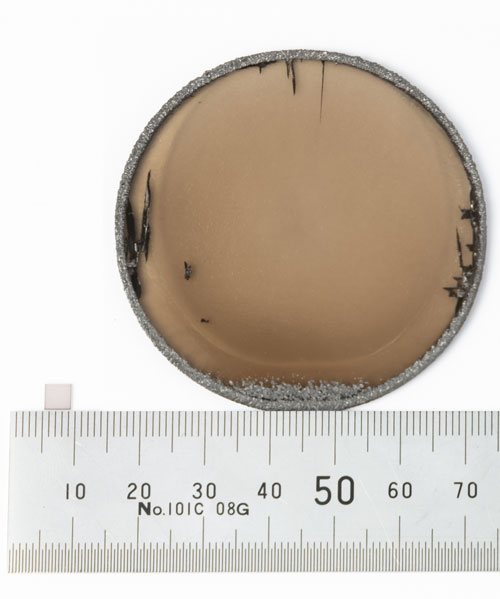
Success in mass production technology for ultra-high-purity 2-inch diamond wafer; expected to spur realization of quantum computing
-
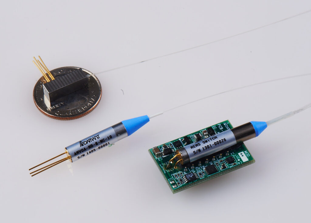
MEMS technology: Backbone of smartphone and optical communications technology
-
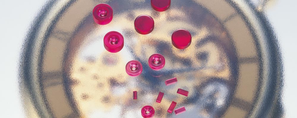
Jewel bearings: Orbray and the watch industry [Story of Watch 1]
-
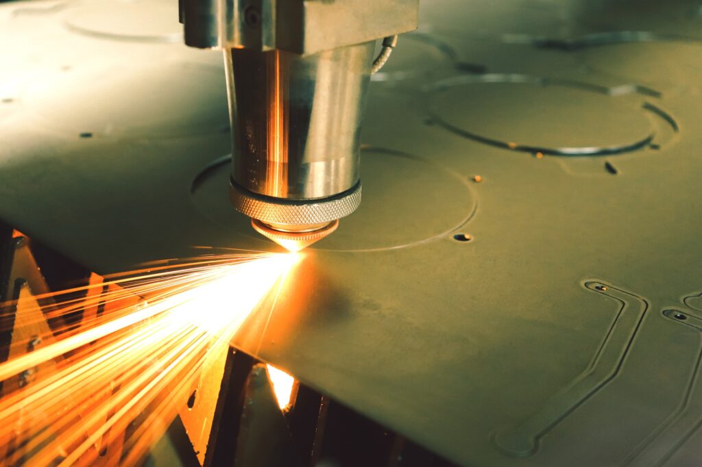
All About Lasers: How they work, their properties, and their uses
-
First round of Space Delivery Project “RETURN to EARTH” The ceremony celebrating the return of the payload items was held

-
Launch of the world's first large12-inch high-quality sapphire wafer