Launch of the world's first large12-inch high-quality sapphire wafer
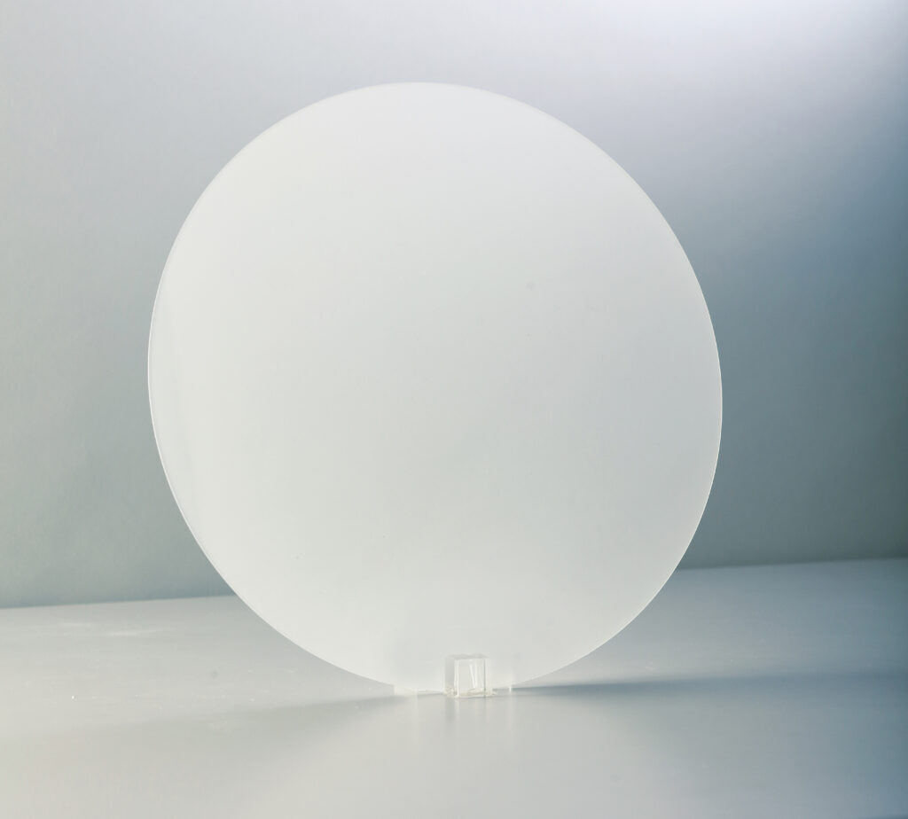
Adamant Namiki Precision Jewel (Adachi-ku, Tokyo; President and CEO: Riyako Namiki) began test sales of large-sized 12-inch(Φ300mm) sapphire wafer.
While sapphire wafer has been used as a base for LED lighting applications, in recent years demand has also been rising for use in the semiconductor industry, which is now interested in large (12-inch) wafers similar to those made of SI (silicon). In anticipation of demand for large (12-inch) sapphire substrates for bonding with silicon substrates, for use as carrier wafers, and for use in epitaxial growth, we have succeeded in producing a 12-inch wafer by leveraging our sapphire wafer manufacturing technology and substantial expertise.
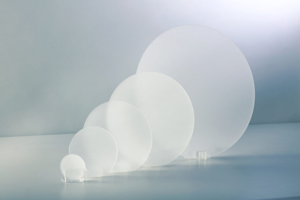
For several years, we have been focusing on the manufacture of sapphire wafers of even higher quality in terms of surface cleanliness, expanded diameter, and shape control, in response to customer needs. We offer epitaxial-quality sapphire wafers from 2 inches to 12 inches in diameter.
- Features
1. The world’s first sapphire wafer of high enough quality for epitaxy.
2. Extremely low contamination from particles or metal contaminants on sapphire wafers with a
diameter of 2 inches to 12 inches.
Prime substrates of 2 inches to 8 inches in diameter, with particle control at the following levels:
-Particle (size≧0.3μm) ≦ 50pcs/2inch
-Metal contaminants (K, Ti, Cr, Fe, Ni, Cu, Zn) ≦ 2E10atoms/㎠
Contaminant control for 12-inch sapphire wafers expected to be equivalent to that for prime
wafers.
3. Concave and convex wafer shape control.
4. Expected applications for 12inch sapphire wafers.
-Substrate for hetero epitaxial growth
-Carrier wafer
-Wafer bonding (e.g., silicon + sapphire)
For more information contact
Adamant Namiki Precision Jewel Co., Ltd. Precision Jewel Division
TEL:+81-3-3919-2200
Related Articles
https://orbray.com/magazine_en/archives/1200
https://orbray.com/magazine_en/archives/1313
https://orbray.com/magazine_en/archives/19
https://orbray.com/magazine_en/archives/11
-
Ceramic substrates and raw materials

-
Precision Nozzles: Materials, Shapes, and Applications
-
What is an audio accessory? An overview and detailed explanation of products [Part 2]

-
MEMS technology: Backbone of smartphone and optical communications technology
-
Introduction to Power Semiconductors: From the basics to applications for each material

-
Space Delivery Project: Return to Earth
Initial shipment launched
Scheduled to return to Earth
after 6 months of exposure to outer space

