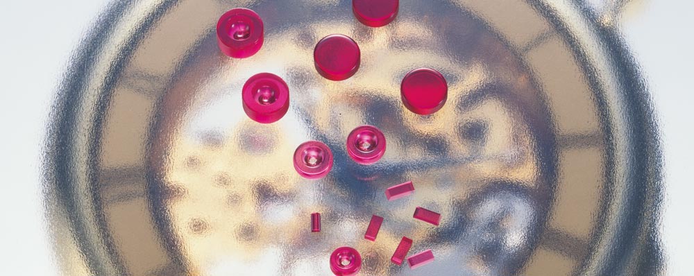
High Flatness Polishing Processing
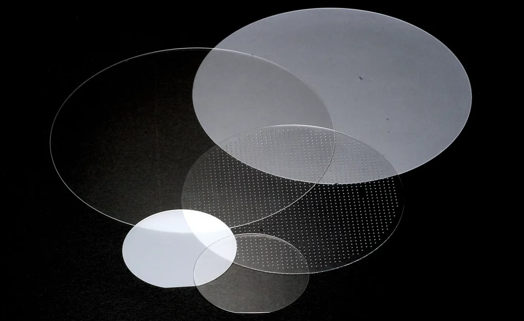
We have a proven track record in mass-production of sapphire wafer for LED, and possess the technology for micro processing and room temperature bonding of sapphire.
Room temperature bonding, in particular, requires materials to be polished to a high degree of flatness in order to bond at room temperature. Our high flatness polishing technology is the unique capability to enable room temperature bonding.
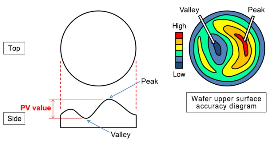
Surface accuracy, which represents flatness, expresses the vertical interval between the highest and lowest points on a substrate, as shown in the figure.
Transparent material with a smaller vertical interval has advantages such as allowing light to penetrate more uniformly or for different materials to be pasted together while maintained the flatness.
By replacing the transparent material with sapphire, one can harness the features of sapphire, such as endurance under high temperature, high thermal conductivity, scratch/crack prevention, and high durability.
In addition to sapphire, we also perform high precision polishing on various other materials by customer request, so please do not hesitate to consult us.
| Materials | Sapphire, Ti sapphire, and other materials |
| Polish system | Single sided polish and double sided polish |
| High flatness polishing on round and square substrates | λ∼λ/20, etc. We consider according to material, size, and shape. |
| Cleaning | Optical grade and epi grade |
| Inspection and evaluation | Interferometer / Zygo and other |
-
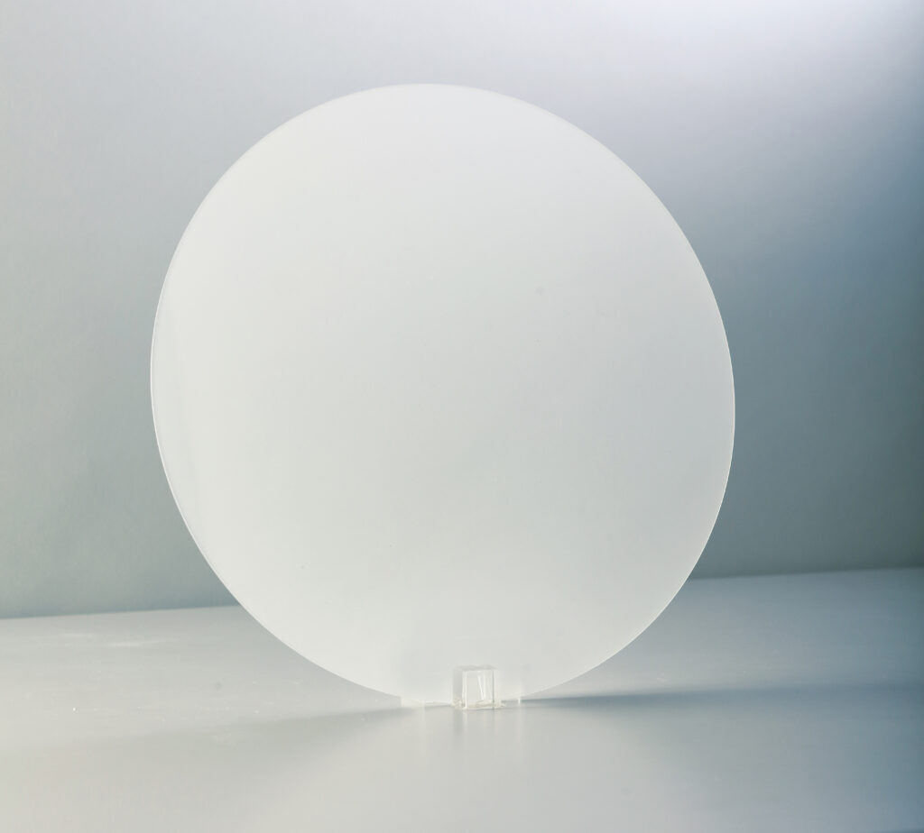
Launch of the world's first large12-inch high-quality sapphire wafer
-
All About Lasers: How they work, their properties, and their uses
-
Precision Nozzles: Materials, Shapes, and Applications
-
The Importance of Chip Mounter Nozzles
-
Diamond Wafers: Production Technologies and Applications
-
Jewel bearings: Orbray and the watch industry [Story of Watch 1]
