Diamond: The Ultimate Material for Next-Generation Semiconductors
Orbray Future ColumnVol.11

Adamant Namiki Precision Jewel Co., Ltd., changed its name to Orbray Co., Ltd., effective January 1, 2023.
View More![]()
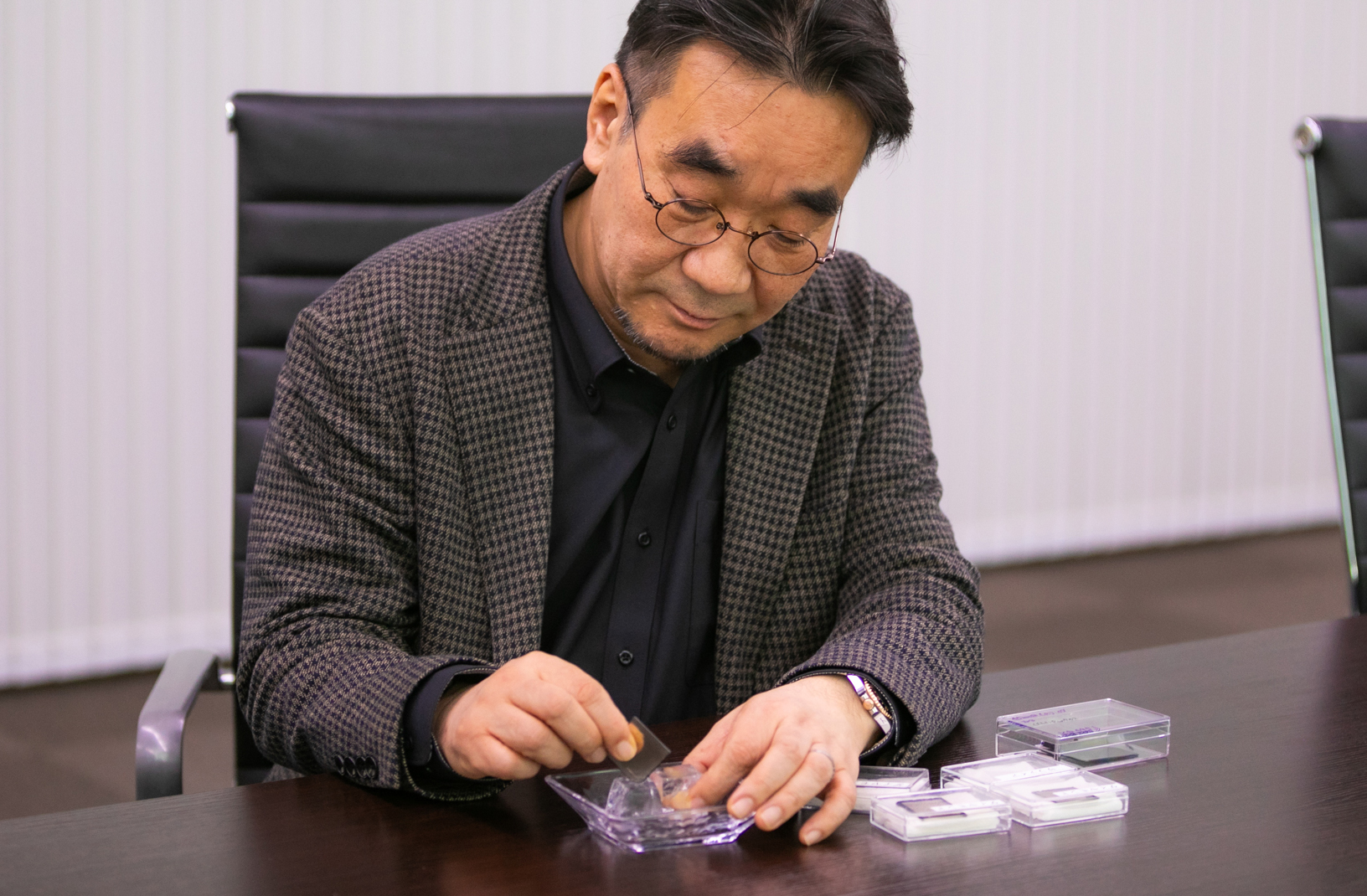
In addition to our other products, diamond and diamond-based products are an important focus for Orbray.
However, these are not the sparkling gemstones commonly associated with the word “diamond.” Instead, we are referring to synthetic diamond engineered for industrial applications. Diamond’s exceptional hardness is essential for Orbray’s advanced processing techniques, such as precision polishing and cutting.
From Industrial Use to Semiconductors: A New Challenge
Our current diamond research focuses beyond traditional industrial applications.
We are now developing methods to grow single-crystal diamond for semiconductor applications. Diamond is often referred to as the ultimate material for semiconductors. Its thermal conductivity and resistance to electric breakdown are far superior to those of silicon, the dominant semiconductor material today. It also outperforms silicon carbide and gallium nitride, which are considered next-generation alternatives. Recognizing this potential, companies worldwide are racing to produce large, flat diamond wafers that can serve as substrates for semiconductor manufacturing.
Bringing Change: The Power of Diamond Semiconductors
Diamond does not transmit electricity; it is an insulator.
For semiconductors to function, they must conduct electricity. Diamond can be made conductive by the introduction of impurities to replace some of the carbon atoms within the diamond crystal. However, precisely controlling the amount of impurity is challenging. Our research focuses on optimizing impurity control to develop high-performance diamond semiconductors.
Conventional semiconductors generate heat when electricity passes through them, requiring cooling mechanisms to prevent thermal damage. Diamond, however, has extremely high thermal conductivity, dissipating heat efficiently. Another limitation of conventional semiconductors is their tendency to break under high electrical loads. To prevent failure, multiple semiconductors are often used to distribute the load. Diamond semiconductors, on the other hand, can handle larger currents and loads with fewer units, making them suitable for compact applications.
Additionally, conventional semiconductors are highly susceptible to radiation, which is why vacuum tubes are still used in satellite applications. Diamond semiconductors are highly resistant to radiation, making them ideal for use in outer space. They are also expected to play a key role in equipment used in high-radiation environments, such as during the decommissioning of nuclear power plants.
Looking Ahead to the Quantum Era
Diamond semiconductors are also gaining attention in the field of quantum computing. Researchers are exploring ways to use diamond to overcome the major technological challenges of the field and develop computers with performance far beyond that of current systems.
However, diamond semiconductors are not yet ready to be commercialized. One of the biggest challenges is the difficulty of producing large synthetic diamond suitable for semiconductor manufacturing.
Orbray Innovates to Meet the Global Challenge
Since establishing the diamond synthesis department at the Yuzawa factory in February 2016, Orbray has been advancing research in collaboration with various universities and research institutes around Japan.

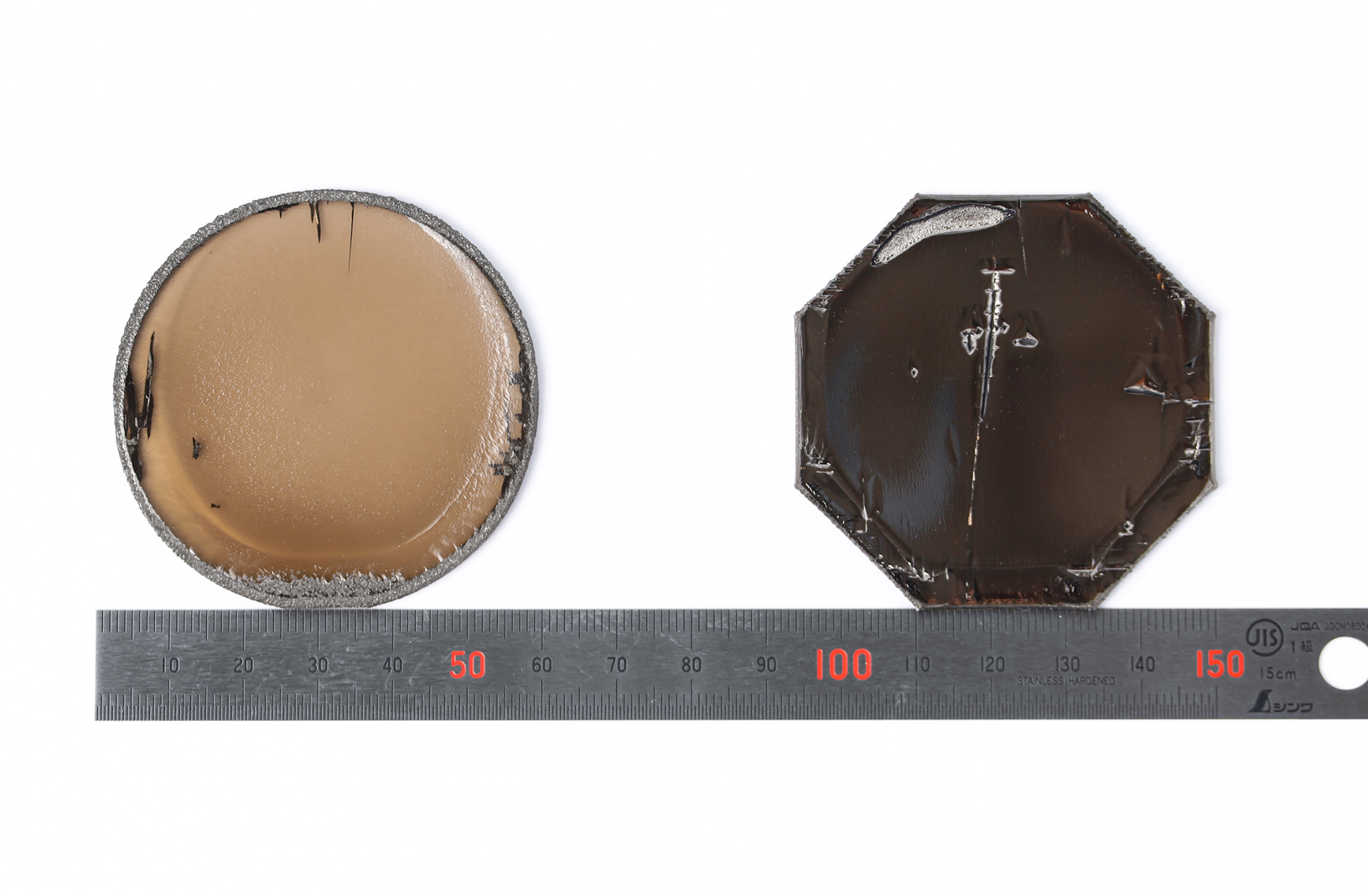
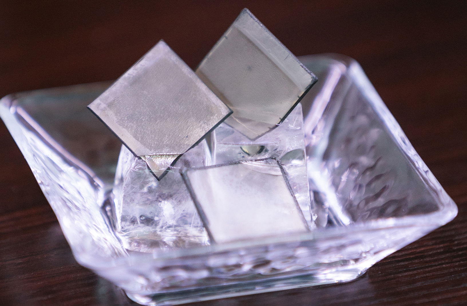
Synthetic diamond is typically grown in a high-temperature furnace by introducing methane and hydrogen gas onto a diamond base. However, using a small base limits the size of the diamond crystals that can be produced.
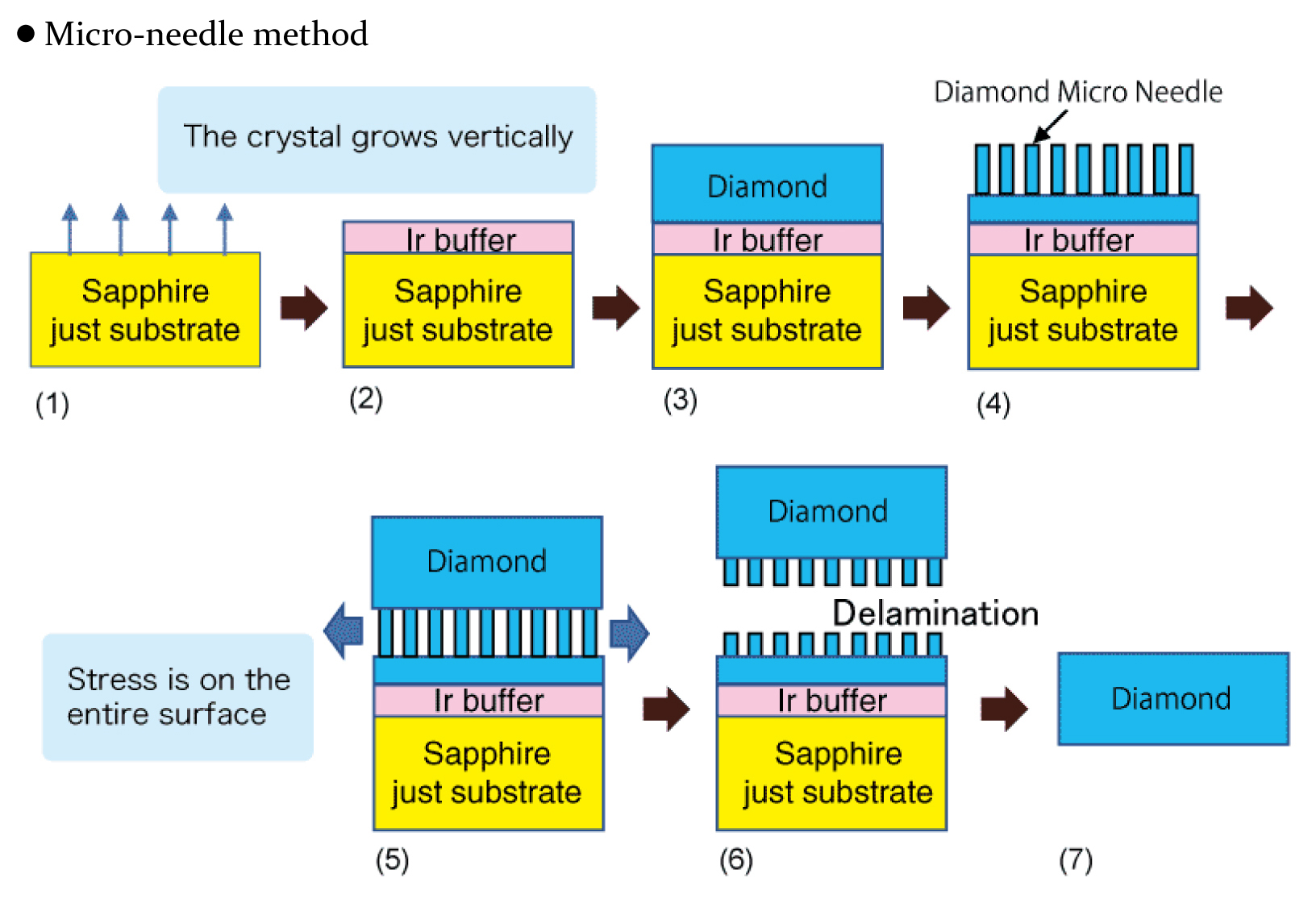
To overcome this challenge, we experimented with using sapphire as the base material. However, due to the difference in thermal expansion coefficients between diamond and sapphire, the diamond crystal formed on top of the sapphire base would crack. To address this, we developed a new method of growing the diamond crystal on sharp micro-needles. This technique involves forming numerous long, high-aspect diamond pillars on an iridium/sapphire substrate and growing the diamond crystal on top of these pillars to create a large, unified wafer.
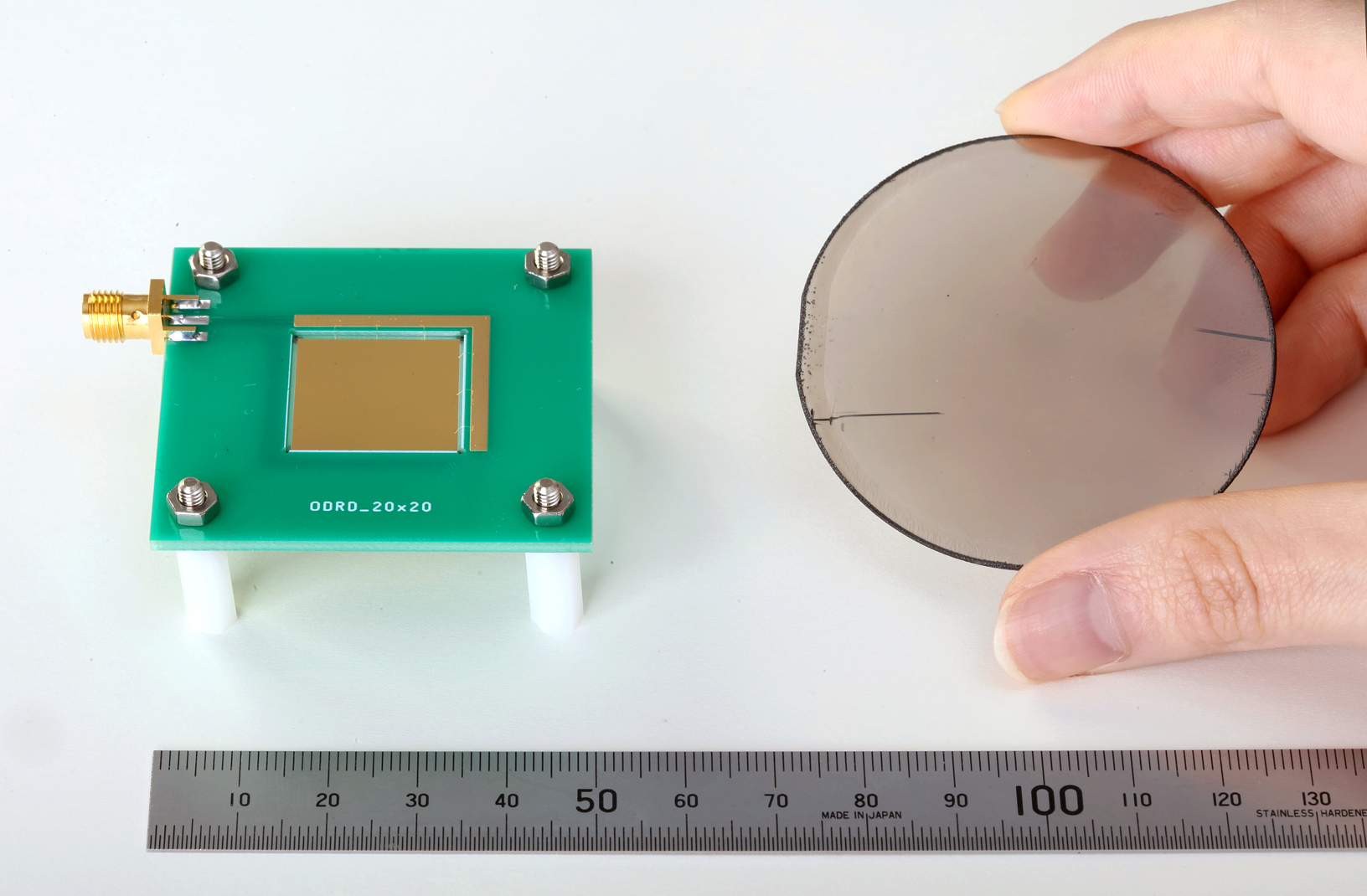
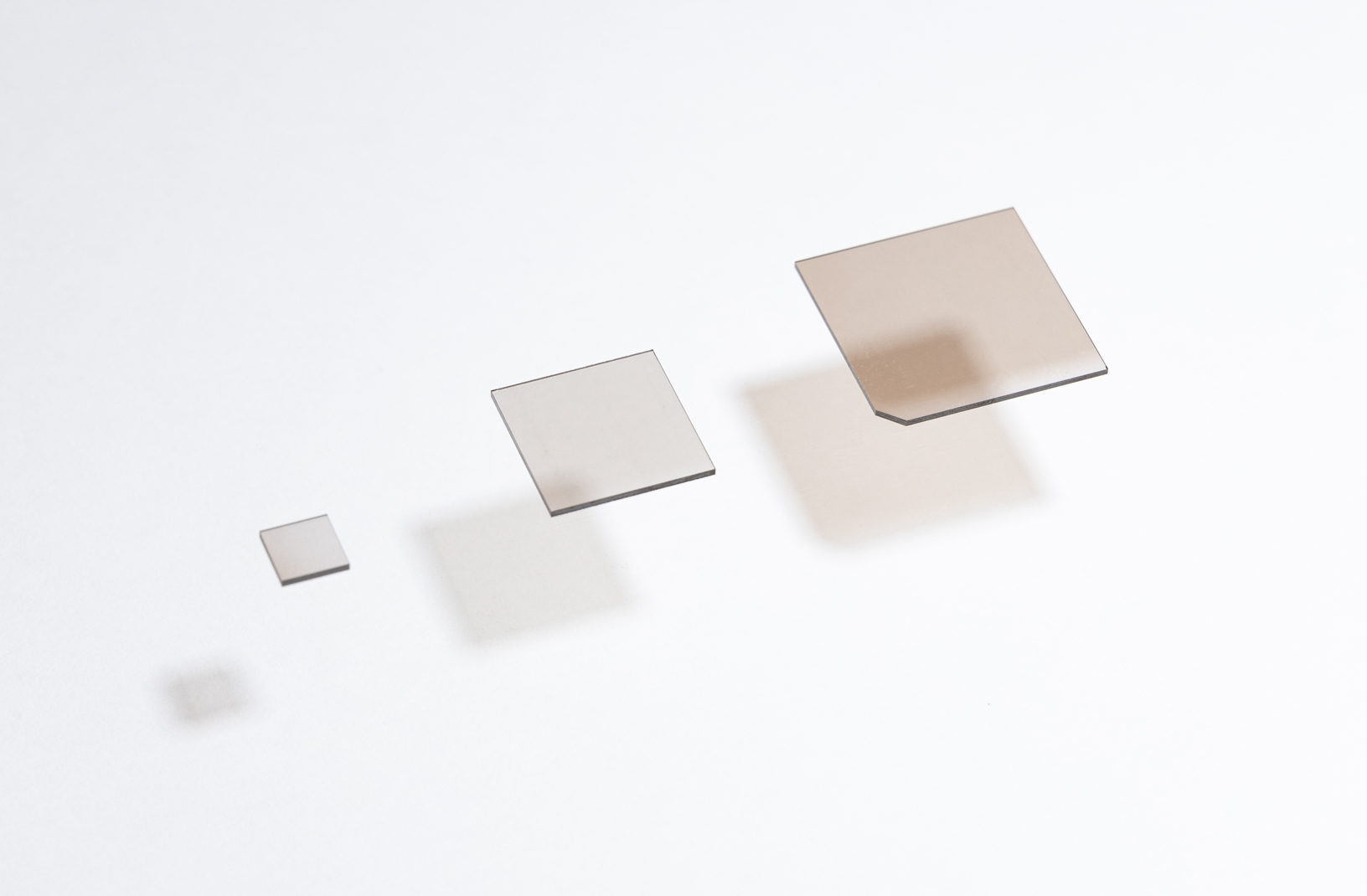
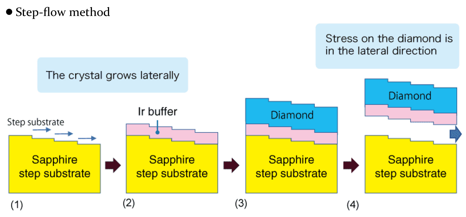
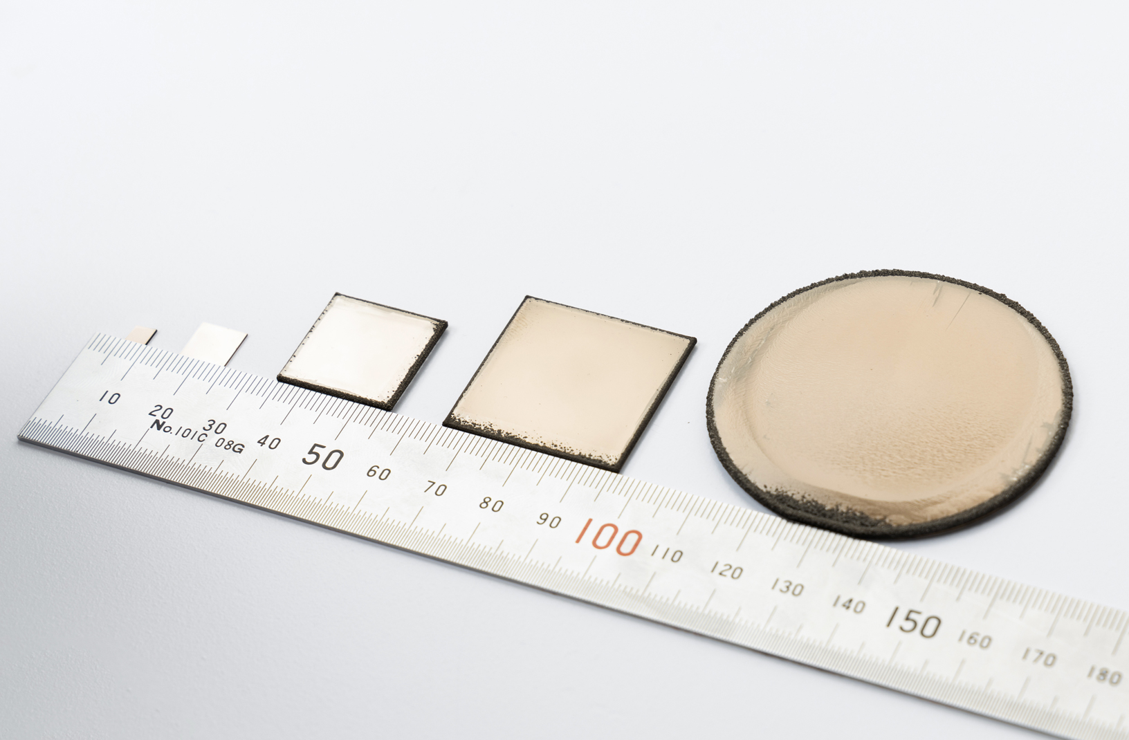
To address the complexity and high cost of the micro-needle method, Orbray developed the step-flow growth method in 2021. This technique reduces defects in diamond substrates by minimizing the stress on the thin diamond film. By growing the crystal on an inclined sapphire substrate, the force exerted on the diamond is significantly reduced. With this method, the diameter of the diamond substrates has been steadily expanded, reaching 2 inches ( 5 cm). Additionally, this breakthrough has led to the development of a mass production process, enabling the creation of higher-quality diamond substrates at a lower cost than ever before.
By tilting the crystalline structure of the substrate by several degrees in relation to the growth plane, step edges on the substrate are created. These step edges become sites for crystal growth and the crystal grows (flows) in the lateral direction, greatly reducing stress and improving the quality of the crystal.
Precision Machining Built on Craftsmanship
Orbray’s synthetic diamond venture is built on decades of expertise in precision jewel parts. To create devices on diamond substrates, the surface must be polished to extremely high precision. However, traditional diamond polishing methods are not suitable for this application. Orbray has therefore developed proprietary polishing techniques specifically designed for diamond substrates. This innovation was made possible through extensive experience in a wide range of diamond applications and a deep understanding of diamond at the atomic level.
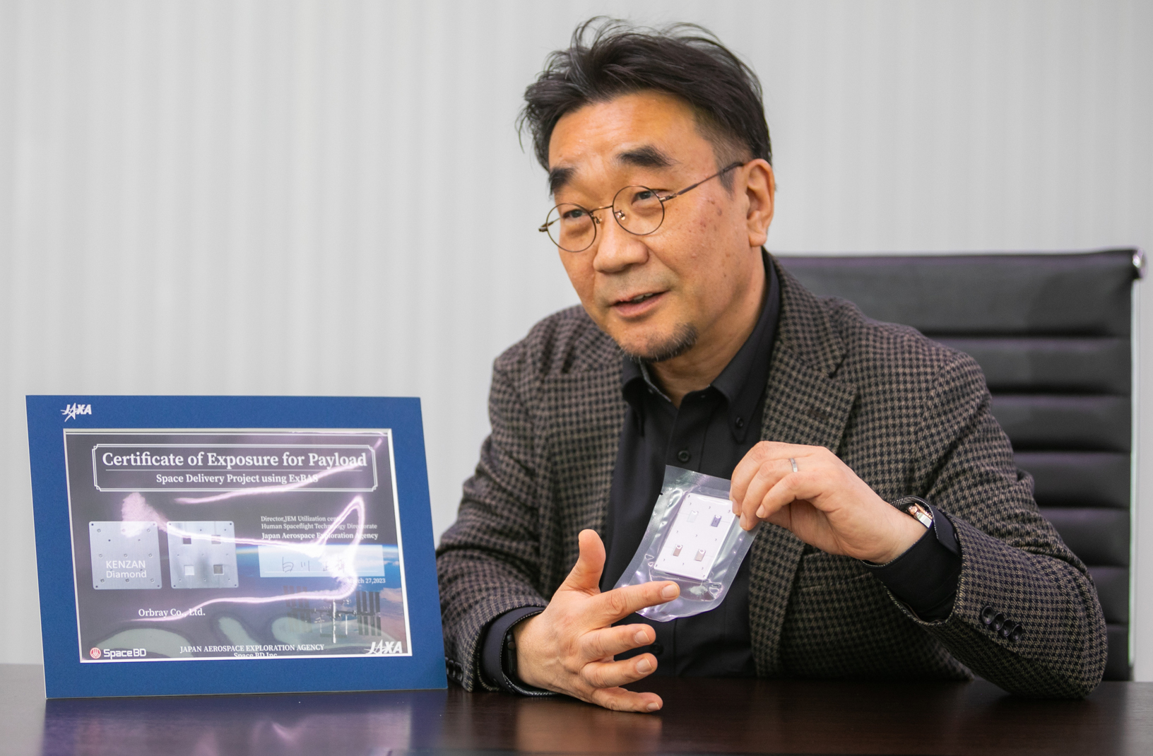
Recognizing the novelty and future potential of these advancements, Orbray was honored as one of the world’s leading synthetic diamond producers. The company received the Semiconductor of the Year award in 2022, from the Electronic Device Industry Newspaper, for its development of industrial production technology for 2-inch diamond wafers.
Creating the future with new collaborations

In June 2023, Orbray launched a joint research initiative with Mirise Technologies, a joint research entity founded by Toyota and Denso to focus on in-vehicle semiconductors. This collaboration aims to develop diamond power semiconductors that offer low power loss and miniaturization, crucial for the advancement of electric vehicles (EVs). These semiconductors are expected to reach the mass market by 2033.
In June 2024, Orbray formed a strategic partnership with Element Six, a global leader in synthetic diamonds and advanced materials. This collaboration aims to produce large-diameter single-crystal diamond substrates of a quality that has not yet been achieved in diamond substrates of 10 mm and larger.
Orbray remains a committed pioneer in synthetic diamond manufacturing, pushing the boundaries of what semiconductors can achieve, and contributing to the advancement of science and technology.