Ceramic substrates and raw materials

What do you think of when you hear, “ceramic substrate”?
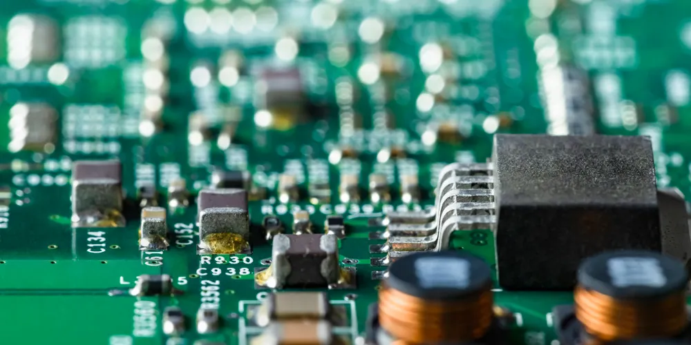
For many, the word “substrate” conjures up images of the green printed circuit boards common in electronic devices. However, ceramic substrates for electronic components have distinct characteristics and applications compared to traditional printed circuit boards.
Ceramic substrates have excellent heat resistance, insulation, and mechanical strength, and play an important role in a wide range of electronic devices, from semiconductor devices to high-frequency circuits.
Table of contents [close]
Types of ceramic substrates and applications
High-temperature ceramic substrates
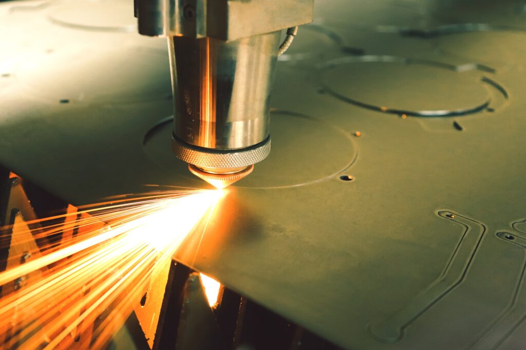
High-temperature ceramic substrates are manufactured using high-temperature co-fired ceramics (HTCC). Materials such as alumina (Al2O3) and aluminum nitride (AlN) that have high thermal conductivity are fired together at temperatures ranging from 1,600 to 1,700℃. To ensure reliability in high-temperature environments, heat-resistant metals like tungsten (W) and molybdenum (Mo) are used for the circuit traces (*1).
*1 Circuit traces are conductive patterns designed to conduct electrical current across the substrate. These patterns are formed on the substrate surface using processes such as etching, printing, or laser machining.High-temperature ceramic substrates offer excellent thermal conductivity and high mechanical strength, delivering stable performance even under demanding conditions. They are ideal for applications that require effective temperature management, including power semiconductor modules and LED packages.
Low-temperature ceramic substrates
Low-temperature ceramic substrates are manufactured using low-temperature co-fired ceramics (LTCC). Glass-based materials are added to alumina and then co-fired at a relatively low temperature of about 900℃. Because of the lower firing temperatures, materials such as silver (Ag) and copper (Cu) – which would degrade or evaporate at temperatures above 1,000°C – can be used for the conductive circuit traces. This results in lower electrical resistance compared to high-temperature ceramic substrates.
These substrates are formed by stacking multiple layers on top of each other. This results in high-precision, high-density circuit designs and enables the miniaturization of electronic devices. In addition, they have thermal expansion coefficients similar to that of silicon (Si), making them well-suited for mounting semiconductor chips.
LTCCs are also resistant to shrinkage, and the size and shape of the substrate can be designed to meet specific customer requirements.
LTCC substrates are particularly well-suited for high-frequency applications such as communication devices, millimeter-wave components, and sensor modules.
Thick-film ceramic substrates
Thick-film ceramic substrates are produced by printing conductor or resistor paste – such as silver or gold-palladium alloys – onto a ceramic base and then repeatedly firing them.
"Thick film" is so called because the conductor or resistor is 10 µm or thicker. This allows flexibility in circuit formation, making these substrates ideal for precision medical devices and automotive components.
Thick-film ceramic substrates have high heat resistance and durability, important qualities for use in high-frequency circuits and power electronics applications.
Other ceramics substrates
There are many other types of ceramic substrates, each with distinct characteristics and applications.
| Type | Features | Application |
| Sapphire substrate | Heat resistance, insulation, mechanical strength | Able to accommodate fine processing. Used in processes that require precise features. |
| Alumina substrate (Al₂O₃ substrate) | Heat resistance, insulation | Used in a wide range of applications, especially in electronics; excels at dissipating heat. |
| Aluminum nitride substrate (AlN substrate) | Thermal conductivity | Used in power devices, LED lighting, laser devices, etc. Ideal when efficient cooling is required. |
| Titanium oxide substrate (TiO₂ substrate) | Heat resistance, insulation | Ideal for high-temperature and high-pressure environments. |
| Silicon nitride substrate (Si₃N₄ substrate) | Mechanical strength, heat resistance | Ideal for use in harsh environments where high mechanical strength is required. |
| Beryllium oxide substrate (BeO substrate) | Thermal conductivity, insulation | Used in power electronics and high-frequency devices. |
| Zirconium oxide substrate (ZrO₂ substrate) | Heat resistance, mechanical strength | Ideal for environments where high wear resistance is required, i.e., aerospace and medical equipment. |
| Corundum substrate | Hardness, heat resistance | Industrial grade heat-resistant materials. |
Ceramic substrates and processing technology
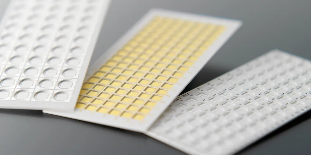
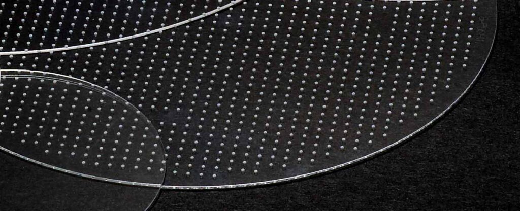
LTCC substrates
Orbray acquired Panasonic’s LTCC operations in 2014. Today, the entire process is carried out in-house, including component mounting onto substrates.
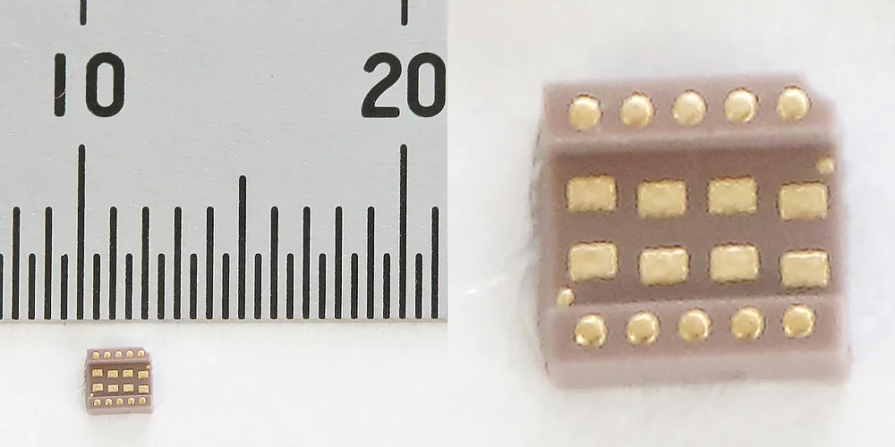
The ability to manufacture high-precision LTCC substrates is one of Orbray’s proprietary technologies.
Through advanced multilayering technology, Orbray is able to integrate multiple electronic components onto a single substrate, making ultra-compact devices possible.
It is also possible to form cavities with an accuracy of 30 µm on a 2 mm square substrate.
In addition to this high precision, Orbray is able to support a wide range of structural variations, from three-dimensional and hollow structures to side surface electrodes. In order to contribute to environmentally friendly solutions, biocompatible materials are selected.
We at Orbray specialize in creating products that are both high-precision and compact.
High-Precision Polishing Technology Developed Through Sapphire Wafer Processing
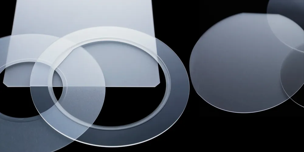
In addition to manufacturing high-precision ceramic substrates, Orbray excels in polishing technologies that enhance the performance of existing ceramic substrates.
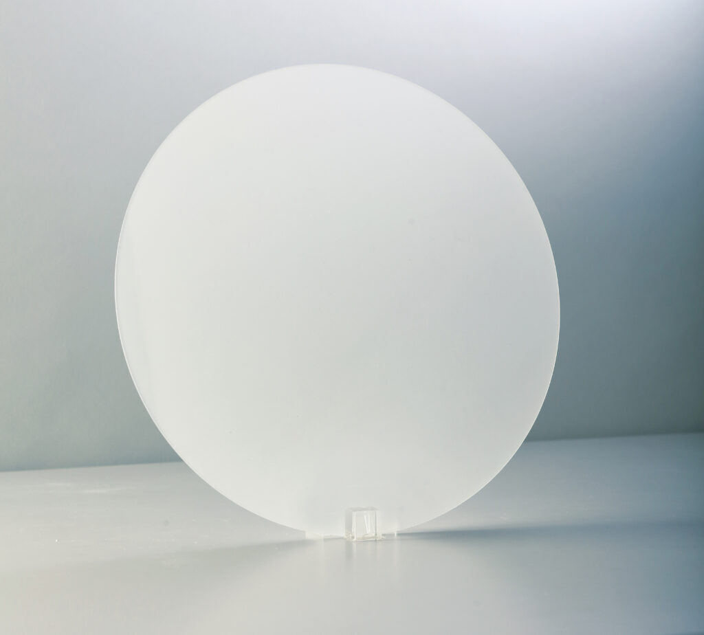
Originally, Orbray specialized in processing sapphire (*2), a single-crystal form of alumina.
*2 Sapphire has long been used for watch crystals and jewelry, and more recently as the substrate material for blue light-emitting diodes (LEDs), which have significantly raised its public profile. Although sapphire offers a stable crystal diameter, its extreme hardness makes it difficult to process.Orbray’s strength lies in its advanced polishing technology, which achieves atomic-level precision to expose the crystal lattice plane of sapphire.
■Sapphire polishing (c-face) – the polishing limit
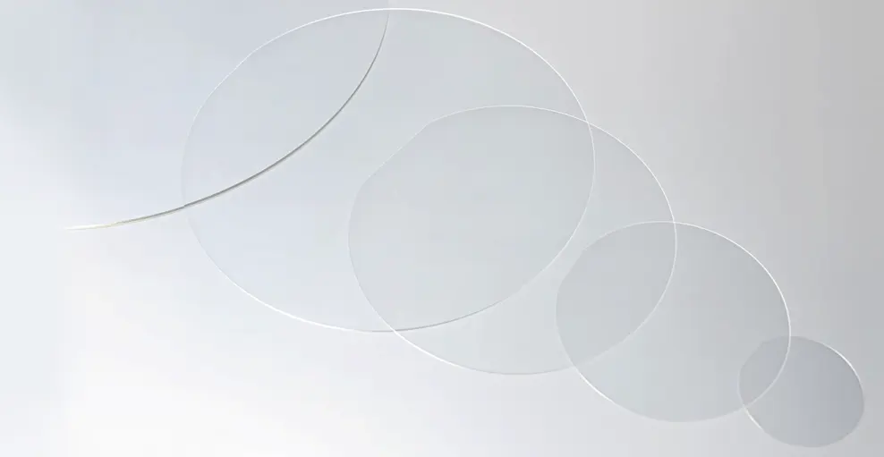
By applying the technology we’ve developed through sapphire processing, namely, polishing hard materials to the nano level, Orbray can produce ceramic substrates with exceptionally high surface smoothness. Substrates with high surface smoothness enable more efficient transmission of electrical signals and contribute to improved device performance.
As noted earlier, ceramic substrates are made by combining and firing multiple inorganic materials. Unlike sapphire, which is a single crystal, ceramic substrates are composite materials.
This makes them more vulnerable to a phenomenon called grain shedding, where improper polishing causes material to crumble and detach from the surface.
Orbray’s advanced polishing techniques help prevent grain shedding while achieving ultra-smooth surfaces.
In practice, after polishing a commercially available ceramic substrate, Orbray was able to achieve an Ra value (an indicator of surface roughness) of just 3.5 nm, demonstrating nano-level smoothness.
By comparison, typical ceramic substrates generally have Ra values ranging from several tens to hundreds of nanometers, further evidence of the high precision of Orbray’s polishing technology.
In addition, such high precision polishing enables the design of more complex circuit patterns, leading to smaller, higher-performance devices.
We also offer custom polishing services on a contract basis for widely used ceramic materials such as Si, SiC, and GaN.
We welcome requests for customized solutions. We look forward to hearing from you about your specific needs.
Related products


-
Color of Jewel
-
Surface polishing technologies - Essential technologies for semiconductor, MEMS, and LED manufacturing
-
All About Lasers: How they work, their properties, and their uses
-
Cut of Jewel
-
Launch of the world's first large12-inch high-quality sapphire wafer
-
What is an audio accessory? An overview and detailed explanation of products