High-quality and Large-diameter Diamond Substrates
In the previous blog installment, we discussed many of the different ways that diamonds, the king of all materials, could enrich our lives in the future. In this article, we will discuss large-diameter diamond substrates, which will be essential for production of the devices of the future.
Table of contents [close]
The need for large-diameter diamond substrates
Most semiconductors used in today’s electronic devices are made out of silicon. Silicon based devices are mass-produced in state-of-the-art fabrication facilities, and continue to evolve day by day. In other words, state-of-the-art semiconductor manufacturing equipment have been designed to extract the highest possible performance out of silicon, and it is able to do so on a mass-production scale. Due to its excellent properties, diamonds are expected to surpass the performance of current semiconductor materials such as silicon, and even surpass those of next generation materials such as SiC and GaN. Mass production of advanced devices appears to be possible if we are able to take advantage of diamond’s excellent properties in the near future. However, manufacturing large diameter diamond substrates has proven to be difficult. As shown in Figure-1, diamonds lag far behind other materials in terms of substrate size. Current silicon wafers are 300 mm in diameter. At less than 50 mm, current diamond wafers are smaller than silicon wafers of 6 generations ago.

Ref: SiC, GaN, and other wide band gap materials for power electronics applications, yole development
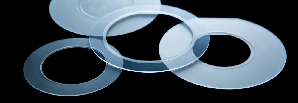
Research is progressing around the world to increase the size of diamond wafers. Orbray has successfully produced 25 mm diamond substrate by the microwave plasma CVD method. We are challenging the production of 50 mm wafer by combining two separate technologies: the heteroepitaxial growth method, and the microneedle method. Each method is discussed in detail below.
Homoepitaxial growth versus heteroepitaxial growth
The microwave plasma chemical vapor deposition method (the CVD method) was explained in a previous article about growing diamonds synthetically. The CVD method requires a base substrate to grow diamonds. The simplest method is to grow diamonds on diamond substrates. This is called homoepitaxial growth. Since the diamond is grown on top of another diamond, there is very little stress and diamonds with good crystallinity and very little distortion can be grown. A high-pressure high-temperature (HPHT) grown diamond is generally used for homoepitaxial growth using CVD method. However, as discussed in the previous article, large diameter diamonds cannot be produced with the HPHT method. In addition, it is very difficult to create diamonds with diameters greater than the seed diamonds themselves by the CVD method. In other words, it is not possible to make large diameter homoepitaxially grown diamond substrates using the CVD method.
Therefore, we attempted to grow diamonds by the CVD method on substrates other than diamonds. This is called heteroepitaxial growth. A metal called iridium is a suitable material. The concept was to embed a large number of minute diamond crystals into the surface of the iridium metal, and grow diamond crystal by the CVD method upon it. The diamond with the same diameter as the substrate should grow on top of the iridium substrate. However, iridium is a precious metal and large diameter iridium substrates are also not available. Therefore, a high-quality iridium thin film was deposited on silicon or sapphire substrates. Minute diamond particles were embedded on the iridium thin film, and diamonds were grown on top with the CVD method to achieve large diameter diamond crystal. The table below summarizes the general characteristics of the homo and heteroepitaxial growth methods.
| HPHT Method (High-temperature high-pressure method) | CVD Method | ||
| Homoepitaxial growth | Heteroepitaxial growth | ||
| Substrate | Diamond | Diamond | Materials other than diamonds (ie: iridium/sapphire) |
| Pros | High crystallinity | Easy to control impurities Low distortion High crystallinity Simple equipment | Easy to control impurities Large diameters possible Simple equipment |
| Cons | Large diameter not possible Slow growth Large, complex equipment | Large diameter not possible (Limited to size of substrate) | High distortion Low crystallinity |
In this article, we will introduce two technologies that we use to overcome some shortcomings of the heteroepitaxial method: distortion and crystallinity.
Orbray is capable of producing high-quality, large-diameter sapphire wafers which are ideal for the formation of iridium thin films. Sapphire is also a very durable material that can easily withstand the severe environment required for the growth of synthetic diamonds. We performed extensive research into the heteroepitaxial growth of diamonds on a iridium/sapphire substrate. However, regardless of the materials chosen for the substrate, the different material properties between the substrate and the diamond resulted in large distortion and low crystallinity. The strain from the distortion was so great that the synthesized diamond (the hardest material on Earth) and the sapphire substrate (the second hardest material on Earth) would sometimes shatter. In order to use the heteroepitaxial growth method, this strain problem had to be overcome. Another key technology, the microneedle method, was developed by Orbray to overcome this issue.
The invention of the microneedle method
We investigated many paths in our attempt to solve the distortion issue seen during the heteroepitaxial growth of diamonds on iridium / sapphire substrates. One idea was to create a cushion between the iridium/ sapphire substrate and the diamond. For this, Orbray invented a diamond microfabrication technique. A nickel thin film was deposited on the surface of the diamond and micro-holes with a diameter of 2 microns were drilled in a regular pattern across the surface in order to expose the diamond. When this was heated to 1000 degrees Celsius in a hydrogen atmosphere, carbon (C) on the diamond that was in contact with the nickel dissolved into the nickel and reacted with the hydrogen (H2) to become methane gas (CH4), which was then exhausted away. By repeating this process, the diamond that was in contact with the nickel was etched away, leaving diamond microneedles 2 microns in diameter and 50 microns high. Although diamond etching with nickel is not a new technology, applying this well-known phenomenon to create elongated diamond microneedles with micron scale diameters is an Orbray original technique.
Figure 3 shows microneedles being used to grow synthetic diamond on a iridium / sapphire substrate. Diamond microneedles were grown on a sapphire substrate which had an iridium thin film. The diamond thick film was grown on the tip of the microneedles at around 1000 degrees Celsius. Due to the different thermal expansion coefficients, when the system is cooled to room temperature, sapphire shrinks quite a bit more than the diamond. This could cause a large degree of distortion. However, this strain was alleviated as the microneedles deflected and finally broke. Since the diamond thick film was spontaneously separated from the iridium / sapphire substrate during cooling down, there was little risk of damage to the diamond during extraction. Furthermore, we have discovered that the microneedles are quite effective in reducing crystalline defects in the growth of the thick film, resulting in high crystallinity of the final product. We named this process the microneedle method.
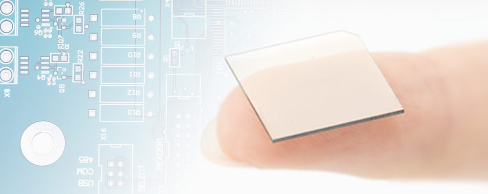
Orbray was able to overcome the strain issues experienced in the heteroepitaxial growth of synthetic diamonds and succeeded in producing a 25 mm diamond substrate at the research scale. A mass production technology for 19 mm diamond substrate has also been developed (see Figure 4). Because the microneedles resemble the needle-point holders used in ikebana called kenzan, we named these diamonds KENZAN Diamond®. Creation of a strong global patent networks is underway with patents already granted in Japan (JP6142145), China (CN105579624), Europe (EP3054036), Korea (KR2016-0065090), and the United States (US2016-237592).
In order to realize a world like the one introduced in the article “The bright future being created by diamonds” Orbray will continue to improve the iridium / sapphire substrate, diamond growing technology, and substrate processing technology, as well as overall substrate size.


-
Award: Industrial Standardization Enterprise Award
-
First round of Space Delivery Project “RETURN to EARTH” The ceremony celebrating the return of the payload items was held

-
Introduction to suction nozzles and collets
-
Silicon Photonics: Why is it essential for 5G?
-
Ultra-Polishing of Sapphire along the c-Plane

-
Industrial applications of sapphire