Power semiconductor for EVs: What are they and what are they used for?
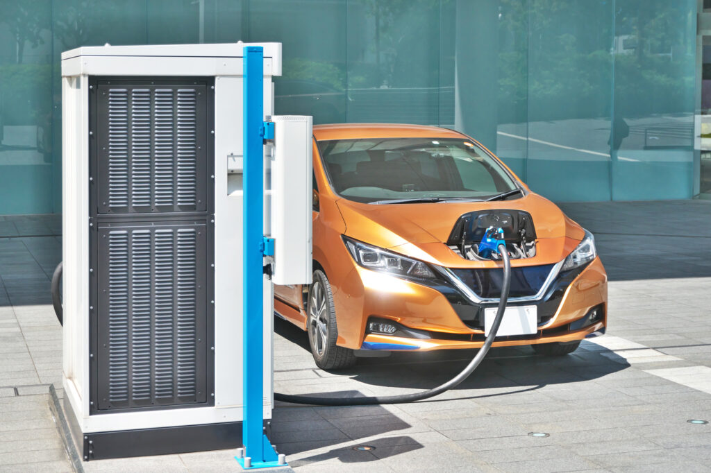
As a solution to global warming caused by excessive release of carbon dioxide into the atmosphere, companies and institutions around the world are developing electric vehicles (EVs). Did you know that power semiconductors play an important role in improving the efficiency and performance of EVs?
This article gives an overview of power semiconductors, what they are used for, and the changes that next-generation power semiconductors will bring.
Table of contents [close]
Overview of power semiconductors and what they are used for

Power semiconductors are expected to improve performance of EVs, by such means as increasing their driving distance and reducing their weight. Here are further details about power semiconductors and how they affect EV performance.
Main parts of EVs
The drive system for moving EVs consists of a battery, a control device, and a motor. DC current generated by the battery is converted in AC current to operate the motor.
More specifically
- The battery produces direct current.
- The DC electricity from the battery is converted into alternating current by the control device.
- The motor uses the AC electricity to rotate, which becomes the driving force for the movement of the EV.
The control device consists of an inverter (an electrical circuit that converts direct current into alternating current) and a converter (an electrical circuit that steps down high-voltage electricity to a lower voltage). The electrical circuits used in control devices operate with large currents and high voltages. Power semiconductors are needed to perform these electrical adjustments.
What are power semiconductors?
Power semiconductors are semiconductor devices that rectify and control electric power. In general semiconductors, power loss occurs, which generates heat. The devices can reach very high temperatures, making them prone to failure.
Power semiconductors differ in that they have been optimized to minimize power loss and dissipate heat quickly. Therefore, they can handle larger currents and higher voltages.
The role of power semiconductors in EVs
Power semiconductors are used in inverters. Specifically, they are used to convert the direct current output from the battery, which is the power source, into alternating current. This is then supplied to the motor that generates the driving force. Since the motor is operated by controlling the output frequency and voltage of the inverter, the vehicle can speed up or slow down based on the inputs from the driver.
Front-end and back-end processes of semiconductor manufacturing
The semiconductor manufacturing process can be broadly divided into front-end processes and back-end processes. The work involved in each differs greatly. They are explained in detail below.
Front-end processes
In the front-end processes, tiny electronic circuits are created on the surface of monocrystal silicon wafers using the following steps.
- Film deposition: Thin films of various materials are deposited on the surface of the silicon wafer.
- Pattern transfer: Circuit patterns are transferred to the thin film by applying photosensitive materials to the thin film.
- Etching: The oxidized portions of the photoresist pattern are etched using specialized chemicals. The remaining material forms the semiconductor circuits.
The semiconductor device is completed by forming a transistor on the bottom layer of the wafer and applying multiple layers of circuitry on top. The various layers that make up semiconductors on a wafer are as follows.
- ・ Element isolation region: The area into which elements that provide transistor functions are doped. High precision is required so the semiconductor can operate without interference from adjacent elements.
- ・ Well: A region on the surface of the wafer into which small amounts of impurities are deposited to form transistors.
- ・ Transistor: A semiconductor element that functions as a switch.
- ・ Electrode: Paths for electricity made of embedded metal to connect the inside of the chip to the outside.
- ・ Wiring layer: A circuit consisting of stacked electrodes and wiring for the electrodes.
Each of these regions and layers is formed by repeating the film deposition, pattern transfer, and etching process. After the formation of the semiconductor is complete, each chip is inspected for performance and quality assurance.
Back-end processes
Back-end processing involves cutting out the semiconductor chips and packaging them into their final forms. The specific steps are as follows:
- Dicing: The semiconductor chips are cut from the silicon wafer.
- Die bonding: The individual chip is placed on a package pedestal and secured with adhesive.
- Wire bonding: The chip is secured onto a metal frame and connected with gold wire.
- Molding: The chip is encapsulated in resin to permanently protect it from contamination and impact.
- Final inspection: Multiple tests are conducted, including for temperature, voltage, and electrical properties, and the external structure is inspected. Items that do not meet standards are removed as defective items.
Semiconductor chips that pass these tests in post-processing are used as final products in various fields, such as EVs and AI.
Changes the next-generation power semiconductors will bring to EVs

What are some of the changes next-generation power semiconductors are expected to bring to the rapidly expanding EV industry? Next-generation power semiconductors are expected to greatly improve the performance of EVs.
What are power semiconductors?
Conventionally, semiconductors, including power semiconductors, have been made of silicon (Si). Research is currently underway to create a next generation of power semiconductors from materials such as silicon carbide (SiC) and gallium nitride (GaN). These materials are expected to bring large improvements in power utilization efficiency.
Research into other high-potential materials such as gallium oxide and diamond is also progressing.
Changes for future EVs
SiC and GaN are attracting attention for use in next-generation power semiconductors. They have a wider energy gap than conventional Si semiconductors, and have a higher dielectric strength than Si.
In addition, these materials reduce switching loss and suppress energy loss due to heat generation, resulting in improved energy efficiency. In addition, the next-generation power semiconductors will require smaller inverters and fewer heat dissipation components. This will lead to reduced manufacturing costs.
Introducing Orbray’s Capillaries
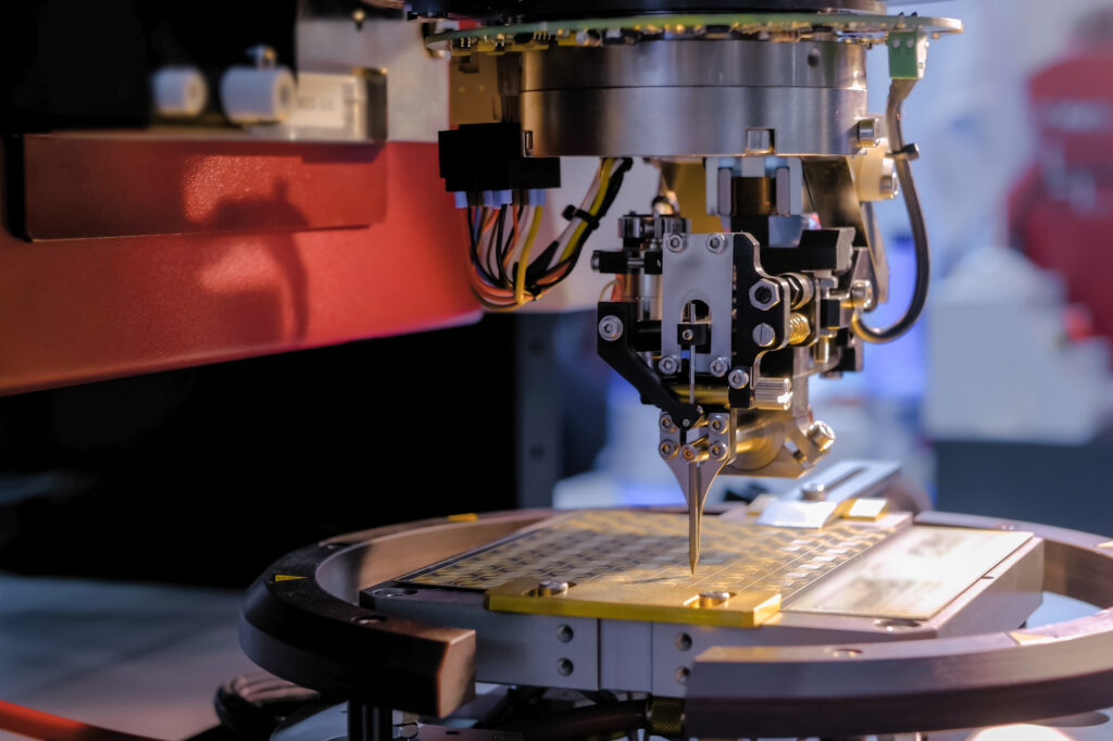
A capillary is a tool used in the bonding step of semiconductor manufacturing. Orbray's ceramic capillaries are manufactured using our injection molding technology. This technology was developed by Orbray to achieve mass production of ferrules in the optical communications field. With our capillaries, the bonding position readjustment time can be reduced when exchanging capillaries. They are characterized by their high hardness and long life.
In addition, since the inner surface of the capillary is polished and has a gentle angle, the bonding shape is highly consistent. The shape of the capillary also reduces damage to the gold wire. Therefore, our capillaries exhibit excellent performance in creating semiconductor packages for EVs.
Summary: Growing attention on power semiconductors
Power semiconductors are essential components of EVs, and the next generation of them is expected to play a major role in reducing power loss and improving heat dissipation. EVs are not their only application. Research is underway around the globe to find ways in which power semiconductors can improve the world around us.
-
Multi-Core Fiber:The highly anticipated, next-generation high-speed communication technology

-
Industrial applications of sapphire

-
MEMS technology: Backbone of smartphone and optical communications technology
-
Orbray Wins Second Consecutive “Semiconductor of the Year” Award in 2023

-
What is a Ferrule? : The history and development of the ferrule continues today with its ever pursuit of high accuracy of 1um or less at reduced costs

-
Award: Industrial Standardization Enterprise Award
