Exposure: The key process that defines semiconductor chip performance

“Exposure” is a crucial process that determines the performance of semiconductor chips.
Photo lithography lies at the heart of this process. Photo lithography systems transfer intricate patterns from a photomask onto silicon wafers with nanometer-level precision. Because of this extreme accuracy, these systems are often described as some of the most precise machines in the world.
Wavelengths of light used for lithography have become shorter over time, from G-rays and I-rays, to KrF, ArF, and now, extreme ultraviolet (EUV) light. Each of these technological breakthroughs enabled further miniaturization of electronic devices. However, challenges such as rising equipment prices and increased production costs have also emerged.
This article provides an overview of lithography (exposure) systems, explores the latest technological trends and current global market share, and highlights the strengths of Japanese companies. Together, these perspectives offer a clear view of the leading edge of the semiconductor industry and the evolution of exposure technology.
Table of contents [close]
Photo Lithography Systems
A lithography system is a semiconductor manufacturing device that draws extremely fine circuit patterns on silicon wafers. The circuit patterns are drawn on what is known as a photomask. The lithography machine projects a reduced image of the photomask pattern onto photosensitive material that has been applied to the silicon wafer, thereby transferring the circuit design. This forms the semiconductor’s circuitry.
These systems are equipped with cutting-edge technology capable of nanometer (one-millionth of one millimeter) precision. This level of precision is indispensable in today’s semiconductor manufacturing. Inside, they integrate advanced optical and control technologies, making them the most sophisticated and expensive equipment in the entire semiconductor manufacturing process.
Different Types of Lithography Systems
How lithography systems work can be understood by examining two key aspects: their operating principles and operation methods.
Different Operating Principles
Lithography systems are generally grouped into four types based on their operating principles.
- Contact lithography
- Proximity lithography
- Projection lithography
- Maskless lithography
In contact lithography, the photomask is placed in direct contact with the wafer surface and exposed to light. This arrangement is simple, and initial costs are low. However, physical contact causes the photomask to wear over time. Because masks must be replaced frequently, running costs are higher. This method was mainly used in the early stages of semiconductor manufacturing.
Proximity lithography is very similar to contact lithography except a slight gap is introduced between the mask and the wafer during exposure. This gap prevents damage to the mask caused by contact. However, resolution is typically lower than in contact lithography.
In projection lithography, lenses or mirrors are used to project a reduced image of the mask pattern onto the wafer. This is the most common method used today for the world’s most advanced chips and uses a wide range of technologies such as ArF immersion and EUV lithography. With an extremely low risk of mask damage, and high yield and throughput, projection lithography is indispensable for leading-edge semiconductor production.
As the name suggests, photomasks are not used in maskless lithography. Instead, electron beams or lasers are used to draw the desired circuit patterns directly onto the wafer. This method achieves extremely high resolution but has slower processing speeds, making it unsuitable for mass production. It is mainly used in photomask fabrication, prototyping, and research applications.
Different Operating Methods
Lithography systems can also be classified by how the image is projected through the mask onto the wafer.
- Stepper Method
- Scanner Method
In the stepper method, a specific area of the wafer is exposed. The wafer is then moved by incremental steps to each subsequent area, and exposure is repeated across its surface. This approach is relatively simple to control and maintains high precision, but because each exposure covers only a limited area, its processing speed tends to be slower.
In contrast, the scanner method projects a slit of light through the mask onto the wafer as both the mask and the wafer move in opposite directions, scanning from right to left during exposure. By precisely scanning small exposure fields, this method can produce uniform patterns over a wide area, making it well suited for mass production of fine circuit patterns.
Technological Trends and Challenges in Lithography
Lithography systems have evolved over the years to produce increasingly finer patterns through shorter wavelengths and larger numerical apertures (NA). However, behind these advances lies a major challenge: the soaring cost of production.
Short wavelengths
The miniaturization of semiconductors has been made possible largely by successive shortening of the wavelengths of the light used for lithography exposure.
In the 1980s, mercury lamps using g-rays (436 nm) were mainstream. These were later replaced by the shorter i-rays (365 nm), improving resolution.
In the 1990s, the introduction of excimer lasers made the use of KrF (248 nm) light sources practical, followed by ArF (193 nm). This enabled pattern formation below 100 nm.
Today, EUV (extreme ultraviolet, 13.5 nm) light is used. This dramatic shortening of the wavelength allows circuits with feature sizes of just a few nanometers.
As light sources have evolved from g-rays and i-rays to KrF, ArF, and now EUV light, the systems used to make the exposure have also become more advanced, providing the basis for continued advancement of the semiconductor industry.
Increasing Numerical Aperture (NA) and Multi-Exposure Technology
The resolution of the lithography system is determined by the formula:
Wavelength ÷ numerical aperture (resolution = λ/NA)
When ArF immersion lithography was mainstream, multiple exposure techniques, such as double patterning, were used to improve the resolution. This made mass production of patterns below 100 nm possible. However, this improvement came with the greater expense of more complex processes and higher production costs.
This was followed by the development of EUV technology, using wavelengths of 13.5 nm, entering into a new era of miniaturization. However, because EUV light is easily absorbed by most materials, conventional refractive lenses cannot be used. Multilayer reflective mirrors are used instead. Achieving an NA of 0.33 under these constraints was made possible through the ultra-precise mirror technology developed by ASML and Carl Zeiss.
Today, development is underway for high-NA EUV systems with an NA of 0.55, a next-generation technology expected to further advance semiconductor miniaturization.
Increasing Production and Equipment Costs
As semiconductor features become ever smaller, the technologies built into lithography systems have become more advanced, resulting in increased production and equipment prices.
In general, shorter wavelengths require more advanced optical systems and tightly controlled internal environments. These physical and technical requirements make the system architectures much more complex, significantly increasing costs.
| Light source (wavelength) | Typical equipment cost |
|---|---|
| i-ray(365 nm) | 500 million JPY ~ |
| KrF(248 nm) | 1 billion JPY ~ |
| ArF Dry(193 nm) | 2 billion JPY ~ |
| ArF Immersion(193 nm) | 6 billion JPY ~ |
| EUV(13.5 nm) | 20 billion JPY ~ |
| High-NA EUV(13.5 nm) | 40 billion JPY ~ |
Before EUV technology was introduced, ArF immersion systems improved resolution through multiple exposures (such as double patterning). However, each additional exposure and photomask increased overall cost. EUV reduces the number of exposure steps but comes with much higher equipment costs—and high-NA EUV generation is even more expensive, exceeding 40 billion yen per system.
Because of its extreme technical requirements, a high-NA EUV system is regarded as an ultra-high-cost piece of equipment, representing the pinnacle of lithography technology.
Global Market Share and Major Manufacturers
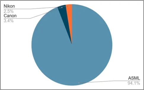
Today’s semiconductor lithography market is dominated by ASML (Netherlands).
Currently, the global lithography market is dominated by ASML, which produces leading-edge machines, while the remaining share is held primarily by two Japanese companies, Canon and Nikon.
ASML is currently the only company in the world that produces state-of-the-art EUV (13.5 nm) lithography systems. It also produces the dominant share of the world’s ArF immersion scanners. This near-monopoly position is the result of its joint development with Carl Zeiss on ultra-precise reflective optics, combined with its highly advanced stage control technology.
In contrast, Japanese manufactures once held roughly 80% of the global market share of lithography systems, but have since fallen far behind ASML. Even so, Nikon and Canon remain key manufacturers in the field of lithography systems.
Lithography Outlook: Roles and Strengths of Japanese Companies
While ASML maintains a virtual monopoly in the production of lithography systems, many of the critical materials, components, and peripheral technologies that enable these systems to operate are supplied by Japanese companies. In particular, Japan plays an essential role in several key areas of EUV lithography within the global supply chain.
| Technology / Industry | Leading Companies |
|---|---|
| Mask Blanks | AGC, HOYA, Shinetsu Chemicals |
| Photoresist | JSR, TOK, Shinetsu Chemicals, Sumitomo Chemicals |
| Coating and Development | Tokyo Electron |
| EUV Mask Inspection | Laser Tec |
These companies have contributed greatly to bringing EUV lithography to practical use.
Although they do not produce the lithography machines themselves, the mass production of semiconductors would not be possible without Japan’s precision engineering and optical materials expertise. Japanese companies also possess strong capabilities in optical components and modules.
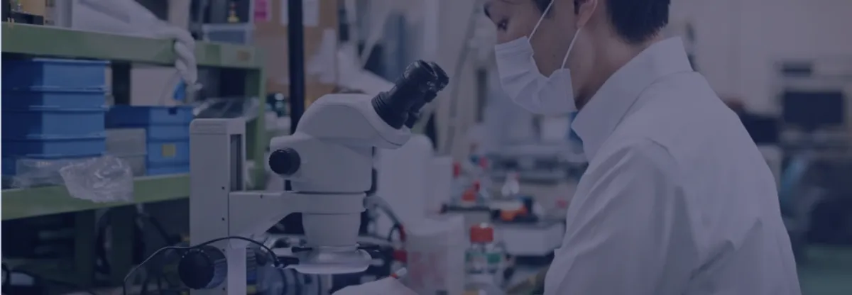
For example, Orbray provides advanced optical solutions through fiber processing, optical module assembly, and optical simulation–based design. With these technologies, Orbray contributes to the ongoing advancement and precision of lithography systems.


Summary: Lithography Integrates Many Advanced Technologies
Through continuous advances in shorter wavelengths, larger numerical apertures (NA), and multiple exposure techniques, circuit patterning at the nanometer scale is now possible. This has been the foundation enabling the evolution of semiconductors and has directly enhanced the performance of devices across industries, from smartphones and automobiles to data servers.
At the same time, new challenges have emerged, including the rising cost of equipment and the increasing complexity of manufacturing processes. Going forward, the industry must continue to balance technological innovation with cost efficiency.
In the next article, we will focus on one of the most notable developments in lithography technology: Direct Imaging (DI) lithography, or maskless exposure systems, and explore how Japanese optical technologies are contributing to their advancement.