Mass production of high-quality, self-standing, large-diameter single-crystal (111) diamond substrates within reach. Development of n-Type Diamonds for Practical Use in Diamond Semiconductors also Making Advances
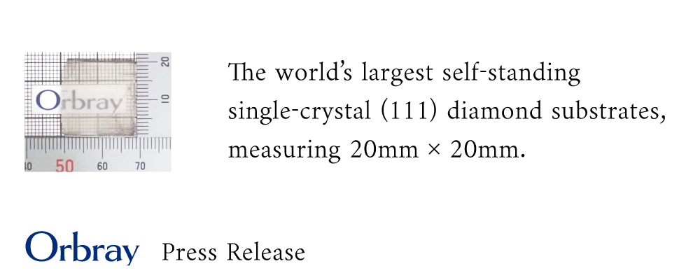
Orbray has developed production technology for the world’s largest self-standing single-crystal (111) diamond substrates, measuring 20mm × 20mm. This achievement marks a significant step in advancing diamond-based quantum devices and power devices. The company aims to commercialize large (111) diamond substrates by 2026 and is also actively working on the development of n-type self-standing diamond substrates, a crucial component for making diamond semiconductor devices mainstream.
Diamond semiconductors are being developed for a wide range of applications due to their exceptional properties. In recent years, there has been significant progress in increasing the size and improving the quality of diamond substrates to meet growing industry demand. High-quality (111) diamond substrates have drawn particular interest in the development of diamond quantum devices*1 that contain nitrogen-vacancy (NV) centers. Additionally, (111) diamond substrates are regarded as essential not only for quantum applications but also for achieving high-performance n-type*2 diamond-based devices, including diamond power devices. However, creating large (111) diamond substrates is difficult and success has been limited. Until now, only small-scale (111) diamond crystals, approximately 3mm square, have been available. Moreover, these crystals were prone to defects known as twin crystals*3, posing significant challenges to the production of large-diameter single-crystal diamond substrates.
In a September 9, 2021 press release, Orbray Co., Ltd., announced the successful development of a high-quality, 2-inch diameter (100) self-standing diamond substrate (product name: KENZAN Diamond™) using its proprietary Step-Flow Growth Method*4. Building on this diamond crystal growth technology and utilizing specially designed sapphire substrates, the company has been advancing the development of a (111) single-crystal diamond self-standing substrate.
This work has culminated in the successful synthesis of a 20mm square (111) single-crystal diamond self-standing substrate without twin defects.
Orbray plans to commercialize this technology by 2026. This advancement is expected to drive progress in the development of diamond semiconductor devices.
Publications related to research results
March 15, 2025, The Japan Society of Applied Physics (JSAP) Spring Meeting: “Large-Diameter (111)-Plane Diamond Free-Standing Crystal Growth”
May 11-15, 2025, International Conference on New Diamond and Nano Carbons: “World-first self-standing (111) heteroepitaxial diamond without twin grown on sapphire substrate”
<Glossary>
*1 Quantum Device
Quantum devices utilize a nitrogen-vacancy (NV) center, a crystal defect in diamond that exhibits atomic-level magnetism (spin). The global race to develop quantum computers and highly sensitive sensors for magnetic fields, temperature, and pressure is accelerating.
*2 n-Type Diamond
Phosphorus-doped diamond semiconductors are key to enhancing the performance of power devices and quantum devices. Reliable semiconductor devices can be created by combining both p-type and n-type semiconductor diamond. However, incorporating phosphorus into (100) single-crystal diamond is challenging. Using the (111) plane makes the process of creating n-type diamond much easier.
*3 Twin Crystals
This is a phenomenon where two or more identical crystals exhibit rotational or mirror symmetry along a specific plane, resulting in an irregular atomic arrangement. In (111) diamond crystals, twin crystals rotated by 180 degrees are more likely to form.
*4 Step-Flow Growth Method
This is Orbray’s proprietary crystal growth technique. Tilting the crystal orientation of the sapphire substrate by several degrees in relation to the A-plane allows creation of a stepped structure at the atomic level for diamond growth. The crystal grows (flows) in a lateral direction across the steps, greatly reducing heteroepitaxial stress and improving the quality of the crystal. (https://orbray.com/magazine_en/archives/811)
*5 Press Release
Success in mass production technology for ultra-high-purity 2-inch diamond wafer; expected to spur realization of quantum computing
https://orbray.com/magazine_en/archives/1401
| About Orbray Co., Ltd. Head Office: 3-8-22 Shinden, Adachi-ku, Tokyo, Japan Established: August 28, 1953 Capital: 100,000,000 JPY Employees: 1000 (January 1, 2025) Founded in 1939 as a manufacturer of precision jewels for bearings used in electricity meters. Through our core technology of Cutting, Grinding, and Polishing, we fuse state-of-the-art technology with master craftsmanship to produce precision jewel parts that are ahead of their time. Currently, we produce precision jewel parts, small DC motors, medical equipment, and other high-tech products. https://www.orbray.com/ |
| 【Contact us regarding this press release】 Orbray Co., Ltd., Diamond Sales Division Substrate Sales Team TEL:+81-3-3919-0101 |