Method for mass production of 2-inch diamond wafers developed - Expected to spur industrialization of power-semiconductor devices
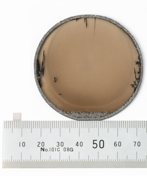
と4mm角のダイヤモンド結晶(左).jpg)
Adamant Namiki Precision Jewel Co., Ltd. (Adachi-ku Tokyo, President and CEO Riyako Namiki) has succeeded in developing a mass production method for 2-inch diamond wafers. The method uses a novel diamond crystal growth technology developed by Adamant-Namiki. 2-inch diamond wafers are vital for semiconductor power device production and this technology is expected to help accelerate research in the field. Adamant-Namiki plans to commercialize the product in 2022.
On April 20, 2021, Adamant Namiki Precision Jewel Co., Ltd., in collaboration with Professor Makoto Kasu of the Faculty of Science and Technology at Saga University, succeeded in producing a 1-inch diameter high-quality diamond wafer (Tradename: KENZAN DiamondTM) using a unique microneedle method*1. Using this wafer, a diamond semiconductor power device functioning on next-generation operating principles achieved the highest levels of high frequency outputs ever recorded*2.
However, industrial research and development of power-semiconductor devices require, at minimum, 2-inch diameter of diamond wafers. Furthermore, the microneedle method developed to create larger diameter wafers added complexity to the manufacturing process, creating a bottleneck for cost reductions.
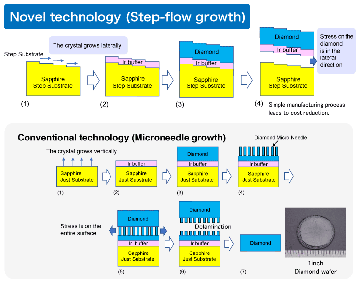
Through independent research, Adamant-Namiki discovered that if sapphire substrates with slightly misoriented surfaces from the A plane were used, diamond crystals could grow with much less strain through a mechanism known as step-flow growth, and large diameter diamond crystals could be produced without the use of microneedles.
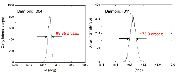
As a result, growth of 2-inch diameter diamond wafers, an essential breakthrough for applications in the electronics industry, was achieved. By measuring the FWHM (full width at half maximum) of the X-ray diffraction rocking curves, the crystal proved to be the highest quality heteroepitaxial diamond crystal ever produced.
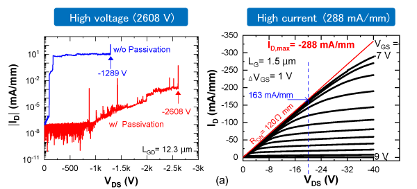
In addition, the diamond-powered semiconductor device made using this wafer succeeded in producing the highest recorded output of 345 MW/cm2.
Adamant-Namiki plans to refine the process in preparation for commercial release in 2022. This should greatly accelerate research of power-semiconductor devices using large-diameter diamond wafers.
Announcement of research results:
82nd SJAP Autumn Meeting 2021
September 13th, 2021
“Heteroepitaxial growth of high-quality diamond crystals using step-flow growth on sapphire substrate” (Presentation number 13a-S301-3)
KENZAN DiamondTM
と4mm角のダイヤモンド結晶(左).jpg)
<Glossary of terms>
*1 Microneedle method
Diamond needles a few micrometers thick and several dozen microns high are fabricated uniformly across the surface of the substrate. The needle layer acts as a buffer as the diamond crystal layer is grown on the needles, and not directly on the substrate, allowing for the formation of 1-inch diameter diamond wafers. However, the added complexity of the process and associated costs were barriers to wide-spread adoption.
Related international papers: S.-W. Kim, Y. Kawamata, R. Takaya, K. Koyama, and M. Kasu, Appl. Phys. Lett. 117, 202102 (2020).
*2 Press Release
Saga University Press Release April 20, 2021: Novel Diamond Semiconductors Operate at Highest Power Ever (https://www.saga-u.ac.jp/koho/press/2021042021534)
*3 Step-flow growth method
By tilting the crystal orientation by several degrees in relation to the C plane of sapphire substrate, step edges on the substrate are created. These step edges become sites for crystal growth and the crystal grows (flows) in the lateral direction, greatly reducing strain and improving the quality of the crystal.
Contact:
Adamant Namiki Precision Jewel Co., Ltd. Relations Office
TEL:+81-3-3919-0101
E-mail:sales@adamant.co.jp
Saga University Public Relations Division
TEL: +81-952-28-8153
Related Articles:
Novel Diamond Semiconductors Operate at Highest Power Ever
World’s First Artificial Diamond Substrate Exposure Experiment in Space
All fields marked with an asterisk * are required.
-
Introduction to winding nozzles: an essential component of the motor coil winding process
-
Success in mass production technology for ultra-high-purity 2-inch diamond wafer; expected to spur realization of quantum computing
-
What is an audio accessory? An overview and detailed explanation of products

-
Orbray Wins Second Consecutive “Semiconductor of the Year” Award in 2023
-
TIME Asia interviewed President Riyako Namiki

-
What is an audio accessory? An overview and detailed explanation of products [Part 2]


