Illustrated guide to semiconductor manufacturing|Step-by-step overview of front-end and back-end processing

From smartphones to automobiles, semiconductors power the devices that play vital roles in our daily lives.
Because semiconductors are highly advanced, their manufacturing processes and technologies are very complex. While many people are familiar with how important semiconductors are, far fewer understand what their internal structures are like and how they are actually made.
This article provides a step-by-step breakdown of the semiconductor manufacturing process, from preparation to final inspection.
Diagrams are provided for each step, so you can follow along and see how semiconductors are made, step by step.
Table of contents [close]
Semiconductor manufacturing | Preparation stage
Semiconductor manufacturing begins with two essential components: the substrate wafer, and the photomask used to limit exposure to light and thereby create circuit patterns. Both are prepared in the initial stage of the process.
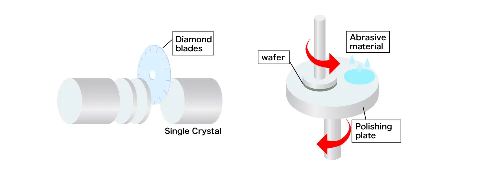
Silicon ingot cutting and polishing
Large blocks of single-crystal silicon, called ingots, are sliced into thin disks using diamond blades or wire saws. Typically, these disks are 200 mm (8 inches) or 300 mm (12 inches) in diameter.
These disks are called silicon wafers and will become the substrate on which semiconductor circuits are created. The wafers are polished to a mirror-like finish so that extremely fine circuits that process information and perform the various functions required of the electronic device can be created on the surface. A complete set of these circuits that is able to perform all of the designed functions is called a “chip.” Hundreds or even thousands of chips can be created on a single 300 mm wafer. Towards the end of the manufacturing process, the wafer is cut apart, or “diced,” to extract the individual chips and package them into semiconductor products.
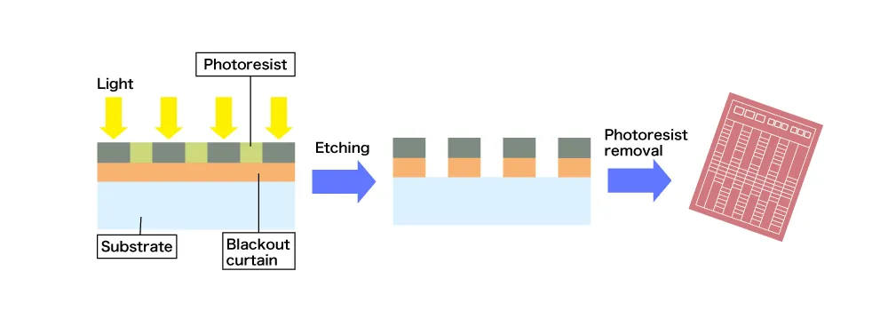
Photomask creation
A photomask is prepared for the “light exposure” step of the manufacturing process.
First, a photosensitive material called photoresist is applied to glass coated with a light-blocking film, such as chrome. The circuit pattern is then drawn onto the surface using an electron beam.
Then, the unwanted photoresist is removed by an etching process. This leaves behind a layer of light-blocking film that matches the design of the desired circuits.
Semiconductor manufacturing | Front-end processing
Semiconductor manufacturing is separated into front-end and back-end processes.
| Front end | Creating circuit patterns on the wafer |
| Back end | Dicing the wafers and finishing the chips so they can be used as semiconductors |
Below is a summary of the 11 front-end processing steps.
1. Wafer surface oxidation
The wafer is placed in an oxidation furnace of around 1,000˚C to oxidize its surface. This creates an oxide film on the wafer that serves as an insulator.
There are two methods, dry oxidation, which uses oxygen, and wet oxidation, which uses water vapor as the oxygen source.
2. Thin film formation
A film with the desired functional characteristics is formed on top of the oxide layer.
Methods such as chemical vapor deposition (CVD), which forms the film through chemical reaction, and physical vapor deposition (PVD), which forms the film by directly depositing materials on the surface, are used for this process.
3. Photoresist application
The photoresist is applied to the surface of the thin film so that the circuit pattern can be drawn by light (“photo”) exposure.
After the photoresist is applied, the wafer is “soft baked” at around 100˚C. This improves adhesion of the film while also removing excess solvent that may be present on the wafer.
4. Exposure
Light is projected onto the wafer through the photomask and lens. This transfers the circuit pattern from the photomask onto the wafer. Shorter wavelength light allows for finer, higher resolution circuit patterns to be drawn.
Currently, argon-fluoride (ArF) excimer lasers with a wavelength of 193 nm (nanometer, or one millionth of a millimeter) are widely used. For shorter wavelengths, extreme ultraviolet (EUV) at 13.5 nm has also been put to practical use.
5. Development
The exposed wafer is immersed in a developer solution to reveal the circuit pattern formed by the exposure.
There are two types of photoresists. In the positive-type photoresist, the exposed areas dissolve away during the development step and the shielded areas remain.
Conversely, in the negative-type photoresist, the exposed areas harden and remain, while the shielded areas are removed by the developer.
6. Etching
The thin film and oxide film are etched away so that only the developed circuit pattern remains.
Wet etching and dry etching processes are used for this step. Wet etching uses an etching solution and is optimal for faster processing. Dry etching bombards the surface with plasma ions. Although it takes more time, dry etching is able to etch more precise patterns.
7. Photoresist removal
After the unneeded oxide film and thin film are etched away, the photoresist is removed. The wafer is then immersed in a chemical solution to remove any remaining impurities.
8. Ion implantation
In its pure state, silicon has low electrical conductivity. For use as a semiconductor, specific ions are implanted, or doped, into the silicon wafer to modify its electrical properties and impart n-type or p-type conductivity to it.
In the periodic table of the elements, silicon is in group 14, and its conductivity is very low. By doping with elements from neighboring groups, the properties of the silicon wafer can be controlled as desired. Doping with group 13 elements creates p-type semiconductors, which provide “holes” that carry a positive charge. Doping with group 15 elements creates n-type semiconductors, which carry a negative charge.
9. Chemical mechanical planarization (CMP)
After an interlayer insulating film is applied, the wafer surface is polished with a pad to make it flat. Planarization creates a smooth surface that allows new layers to be formed on top.
The steps from “photoresist application” through “planarization” are repeated several times to build a multilayer structure with the desired circuit design. Depending on the design of the layer, “ion implantation” may be omitted.
10. Electrode creation
Metal for electrode wiring is embedded in the wafer surface to electrically connect the inside of the device with the outside. This step allows the semiconductor chips created on the wafer to function as a completed circuits.
11. Inspection
A specialized tool called a probe is used to make sure each chip on the wafer is working correctly. Although further inspection is performed during back-end processing, this step helps identify and eliminate defective chips early. Chips determined to be defective are physically or electrically marked so they can be easily removed in the later processing steps.
Semiconductor manufacturing | Back-end processing
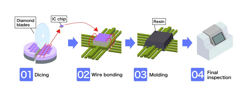
During back-end processing, the semiconductors created on the wafer are cut out into individual chips. The chips are further processed so that they can be used as electronic components in various devices.
1. Dicing
Diamond blades or lasers are used to cut out the individual chips from the wafer. To prevent scattering during cutting, the back side of the wafer is secured with tape.
Physical cutting with a diamond blade is the most common method. Sometimes, lasers or plasma are used to minimize damage to the chips.
The diced chips are transferred to a substrate with suction nozzles or collets.
2. Wire bonding
Each chip is fixed to a substrate, and its electrodes are connected to the lead frame terminals with fine wires, typically gold or copper.
This process requires various bonding tools, such as capillaries for positioning the wires and tensioners for maintaining proper wire tension.
Wire bonding creates the electrical connections that act as the interface with outside circuits, allowing the chip to function as an electronic component.
3. Molding
To protect the chip from external impact and damage, it is encapsulated in specialized resin.
Semiconductors contain many delicate parts and are highly susceptible to impact, so care must be taken to protect them from physical damage.
For example, wire bonding uses ultra-fine gold wires of about 25 µm (micrometer, or one thousandth of a millimeter) in diameter. Encapsulating the chip with resin protects these fragile connections and increases durability.
4. Final inspection
Once the semiconductor is complete, it undergoes multiple tests:
| Test Name | Purpose |
|---|---|
| AC Test | Evaluates timing and AC current characteristics |
| DC Test | Evaluates current, voltage, and other DC current performance |
| Functionality Test | Confirms that the chip operates according to specifications |
| Visual Inspection | Checks for cracks, chips, or other visible defects |
These tests cannot be completed all at once. Depending on the product, hundreds or even thousands of test items are required. Only semiconductor chips that pass every test are packaged and shipped.
Summary | The 15 steps of semiconductor manufacturing
Beginning with wafer and photomask preparation, and continuing through front- and back-end processing, 15 steps are required to create semiconductors.
Each step is carried out to nanometer precision. This highlights the extremely advanced technology required.
The miniaturization of semiconductors means many of the components and features are not visible to the naked eye, so specialized equipment is essential. Some of the systems used in this process demand such a high level of technology that their cost can reach hundreds of billions of yen.
In our next article, we will take a closer look at lithography equipment – the most advanced and most expensive class of semiconductor manufacturing equipment.